CS5460-BS Ver la hoja de datos (PDF) - Cirrus Logic
Número de pieza
componentes Descripción
Lista de partido
CS5460-BS Datasheet PDF : 34 Pages
| |||
CS5460
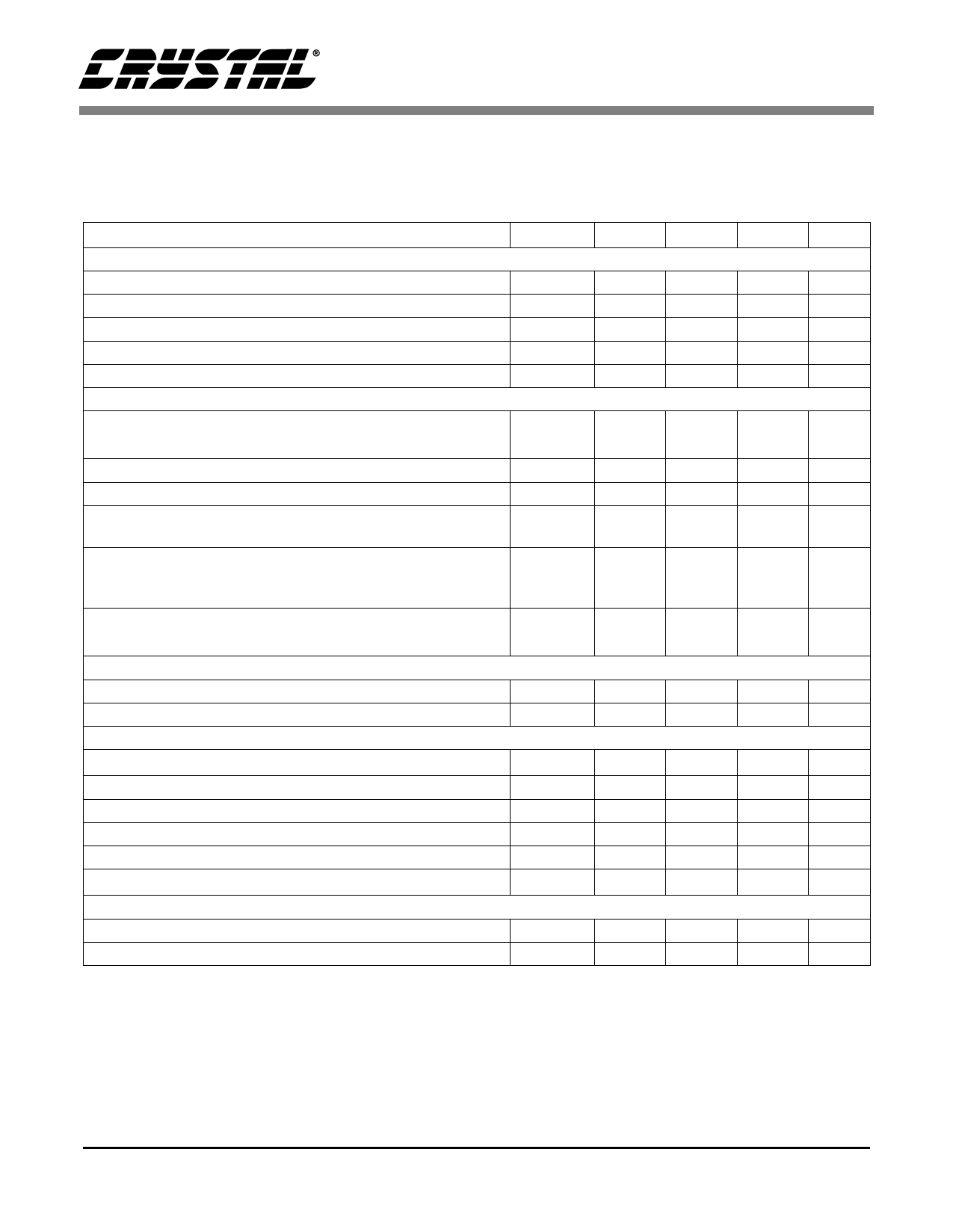
1. CHARACTERISTICS AND SPECIFICATIONS
ANALOG CHARACTERISTICS (TA = -40 °C to +85 °C; VA+, VD+ = +5 V ±10%; VREFIN = 2.5 V;
VA- = AGND; MCLK = 4.096 MHz, K = 1; N = 4000, OWR = 4.0 kHz.)(See Notes 1, 2, and 3)
Parameter
Accuracy (Both Channels)
Total Harmonic Distortion
Common Mode Rejection
(DC, 50, 60 Hz)
Offset Drift (Without the High Pass Filter)
Full Scale DC Calibration Range
(Note 4)
Input Sampling Rate
DCLK = MCLK/K
Analog Inputs (Current Channel)
Differential Input Voltage Range {(IIN+) - (IIN-)} (Gain = 10)
(Gain = 50)
Symbol
THD
CMRR
FSCR
IIN
Common Mode + Signal on IIN+ or IIN- (Gain = 10 or 50)
Crosstalk with Voltage Channel at Full Scale (50, 60 Hz)
Input Capacitance
(Gain = 10) IC
(Gain = 50)
Effective Input Impedance
(Note 5) EII
(Gain = 10)
(Gain = 50)
Noise (Referred to Input)
(Gain = 10)
(Gain = 50)
Accuracy (Current Channel)
Bipolar Offset Error
(Note 1)
Full-Scale Error
(Note 1)
Analog Inputs (Voltage Channel)
Differential Input Voltage Range
{(VIN+) - (VIN-)}
Common Mode + Signal on VIN+ or VIN-
Crosstalk with Current Channel at Full Scale (50, 60 Hz)
Input Capacitance
Effective Input Impedance
(Note 5)
Noise (Referred to Input)
Accuracy (Voltage Channel)
Bipolar Offset Error
(Note 1)
Full-Scale Error
(Note 1)
VOS
FSE
VIN
IC
EII
VOS
FSE
Min
Typ
Max Unit
74
-
-
dB
80
-
-
dB
-
5
-
nV/°C
25
-
100 %F.S.
-
DCLK/4
-
Hz
-
150
-
30
-0.25
-
-
-
-
5
-
25
30
-
30
-
-
-
-
-
-
-
VA+
-115
-
-
mVrms
mVrms
V
dB
pF
pF
-
kΩ
-
kΩ
20
µVrms
4
µVrms
-
-
±0.001 %F.S.
-
-
±0.001 %F.S.
-
150
-0.25
-
-
-
-
0.2
5
-
-
-
-
mVrms
VA+
V
-70
dB
-
pF
-
MΩ
250 µVrms
-
-
±0.01 %F.S.
-
-
±0.01 %F.S.
Notes: 1. Applies after system calibration
2. Specifications guaranteed by design, characterization, and/or test.
3. Analog signals are relative to VA- and digital signals to DGND unless otherwise noted.
4. The minimum FSCR is limited by the maximum allowed gain register value.
5. Effective Input Impedance (EII) varies with clock frequency (DCLK) and Input Capacitance (IC)
EII = 1/(IC*DCLK/4)
4
DS279PP5
Share Link: 