M37640E8 Ver la hoja de datos (PDF) - MITSUBISHI ELECTRIC
Número de pieza
componentes Descripción
Lista de partido
M37640E8 Datasheet PDF : 172 Pages
| |||
Mitsubishi Microcomputer
7600 Series
M37640E8-XXXF Preliminary Specification
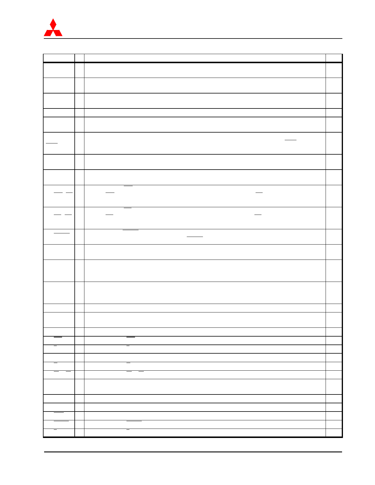
Table 1-2. Pin Description
Name I/O
Description
Pin #
P00/AB0
~ P17/AB15
P20/DB0
~ P27/DB7
P30/RDY
I/O
CMOS I/O
function as
port (address bus).
the address bus.
When
the
MCU
is
in
memory
expansion
or
microprocessor
mode,
these
pins
I/O
CMOS I/O
function as
port (data bus). When the MCU is in memory expansion or
the data bus. These pins may also be used to implement the
microprocessor mode, these
Key-on Wake up function.
pins
I/O
CMOS I/O port (Ready). When the MCU
as RDY (hardware wait cycle control).
is
in
memory
expansion
or
microprocessor
mode,
this
pin
functions
56-41
64-57
40
P31
I/O CMOS I/O port.
39
P32/(VRFY)
I/O
CMOS I/O
verify).
port.
When
the
MCU
is
in
EPROM
program
mode,
the
pin
is
used
as
VRFY
(EPROM
memory
38
P33/DMAout
/PGM
CMOS I/O port (DMAout). When the MCU is in memory expansion or microprocessor mode, this pin is set to a
I/O “1” during a DMA transfer. When the MCU is in EPROM program mode, the pin is used as PGM (EPROM
memory program).
37
P34/Φout
I/O
CMOS
pin.
I/O
port
(Φ).
When
the
MCU
is
in
memory
expansion
or
microprocessor
mode,
this
pin
becomes
Φout
36
P35/SYNCout
I/O
CMOS I/O port (SYNC output). When the MCU is in memory expansion or microprocessor mode, this pin
becomes the SYNCout pin.
35
CMOS I/O port. (WR output). When the MCU is in memory expansion or microprocessor mode, this pin
P36/WR/(CE) I/O becomes WR. When the MCU is in EPROM program mode, the pin is used as CE (EPROM memory chip
34
enable).
CMOS I/O port. (RD output). When the MCU is in memory expansion or microprocessor mode, this pin
P37/RD/(OE) I/O becomes RD. When the MCU is in EPROM program mode, the pin is used as OE (EPROM memory output
33
enable).
P40/EDMA
I/O
CMOS I/O port (EDMA: Expanded Data Memory Access).
microprocessor mode, this pin can become the EDMA pin.
When
the
MCU
is
in
memory
expansion
or
24
P41/INT0
~ P42/INT1
P43/CNTR0
I/O
CMOS I/O
active high
port or
or low.
external
interrupt
ports
INT0
and
INT1.
These
external
interrupts
can
be
configured
to
be
CMOS I/O port or Timer X input pin for pulse width measurement mode and event counter mode or Timer X
I/O output pin for pulse output mode. This pin can also be used as an external interrupt when Timer X is not in
output mode. The interrupt polarity is selected in the Timer X mode register.
23-22
21
CMOS I/O port or Timer Y input pin for pulse period measurement mode, pulse H-L measurement mode and
P44/CNTR1 I/O event counter mode or Timer Y output pin for pulse output mode. This pin can also be used as an external
20
interrupt when Timer Y is not in output mode. The interrupt polarity is selected in the Timer Y mode register.
P50/XCin I/O CMOS I/O port or XCin.
P51/Tout/
XCout
I/O CMOS I/O port or Timer 1/2 pulse output pin (can be configured initially high or initially low), or XCout.
P52/OBF0 I/O CMOS I/O port or OBF0 output to master CPU for data bus buffer 0.
P53/IBF0 I/O CMOS I/O port or IBF0 output to master CPU for data bus buffer 0.
P54/S0
I/O CMOS I/O port or S0 input from master CPU for data bus buffer 0.
P55/A0
I/O CMOS I/O port or A0 input from master CPU.
P56/R(E) I/O CMOS I/O port or R(E) input from master CPU.
P57/W(R/W) I/O CMOS I/O port or W(R/W) input from master CPU.
P60/DQ0
~ P67/DQ7
USB D-
I/O CMOS I/O port or master CPU data bus.
I/O USB D- voltage line interface, a series resistor of 33 Ω should be connected to this pin. (see note)
USB D+
I/O USB D+ voltage line interface, a series resistor of 33 Ω should be connected to this pin. (see note)
12
11
8
7
6
5
4
3
2-1,
80-75
71
70
P70/SOF I/O CMOS I/O port or USB start of frame pulse output, an 80 ns pulse outputs on this pin for every USB frame.
69
P71/HOLD I/O CMOS I/O port or HOLD pin.
68
P72/S1
I/O CMOS I/O port or S1 input from master CPU for data bus buffer 1.
67
Pin Description and Layout
6/2/98
1-7
Share Link: 