CDP1020 Ver la hoja de datos (PDF) - Intersil
Número de pieza
componentes Descripción
Lista de partido
CDP1020 Datasheet PDF : 23 Pages
| |||
CDP1020
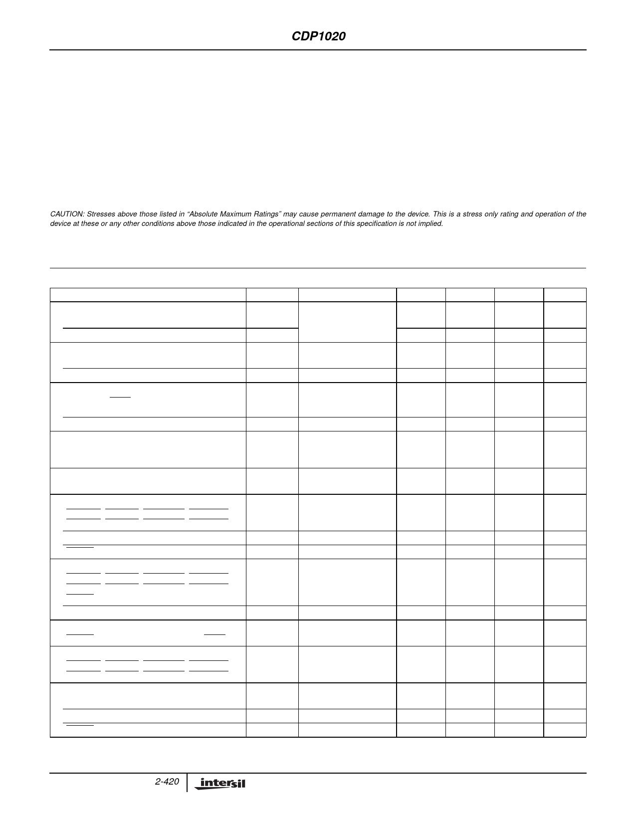
Absolute Maximum Ratings
Supply Voltage, VDD . . . . . . . . . . . . . . . . . . . . . . . . . . -0.5V to +6V
Supply Voltage, VGATE . . . . . . . . . . . . . . . . . . . . . . . . . VDD to 13V
Supply Voltage, VLED . . . . . . . . . . . . . . . . . . . . . . . . . -0.5V to +6V
Input Voltage, VIN . . . . . . . . . . . . . . . . . . VSS - 0.3V to VDD + 0.3V
Test Mode, VIN . . . . . . . . . . . . . . . . . . . . VSS - 0.3V to 2 x VDD + 0.3V
Current Drain Per Pin Excluding VDD and VSS, I . . . . . . . . . . 40mA
Thermal Information
Thermal Resistance (Typical, Note 1)
θJA (oC/W)
28 Ld SOIC . . . . . . . . . . . . . . . . . . . . . . . . . . . . . . .
60
Maximum Junction Temperature . . . . . . . . . . . . . . . . . . . . . . .150oC
Maximum
Maximum
Storage Temperature Range (TSTG)
Lead Temperature (Soldering 10s) .
.
.
.
.
.
.
.
.
-65oC to 150oC
. . . . . . . .300oC
(SOIC - Lead Tips Only)
Operating Conditions
Voltage Range . . . . . . . . . . . . . . . . . . . . . . . . . . . . . +3.0V to +5.0V
Temperature Range . . . . . . . . . . . . . . . . . . . . . . . . . . . 0oC to 85oC
Input High Voltage . . . . . . . . . . . . . . . . . . . . . . . (0.8 x VDD) to VDD
CAUTION: Stresses above those listed in “Absolute Maximum Ratings” may cause permanent damage to the device. This is a stress only rating and operation of the
device at these or any other conditions above those indicated in the operational sections of this specification is not implied.
NOTE:
1. θJA is measured with the component mounted on an evaluation PC board in free air.
DC Electrical Specifications, 5.0V VDD = 5.0V ±10%, TA = 0oC to 85oC
PARAMETER
SYMBOL
CONDITIONS
Output Voltage
All Outputs
SFTLOCK0, SFTLOCK1
Output High Voltage
VOL
VOH
-10µA < ILOAD < 10µA
LEDA0, LEDG0, LEDA1, LEDG1
SFTLOCK0, SFTLOCK1
Output Low Voltage
VOH
VOH
ILOAD = -16.0mA
ILOAD = -0.7mA
SCK, SDA, ALRT, SFTLOCK0, SFTLOCK1,
LEDG0, LEDA0, LEDG1, LEDA1
PWREN0, PWREN1
VOL
ILOAD = 1.6mA
VOL
ILOAD = 60µA
Gate Output High Voltage
PWREN0, PWREN1
VGOH
ILOAD < 10µA
Gate Output Current Source
PWREN0, PWREN1
Input High Voltage
1394PR0, USBPR0, REMREQ0, SECURE0,
1394PR1, USBPR1, REMREQ1, SECURE1
SCK, SDA
RESET, CLK
Input Low Voltage
1394PR0, USBPR0, REMREQ0, SECURE0,
1394PR1, USBPR1, REMREQ1, SECURE1,
RESET, CLK
SCK, SDA
Input/Output Leakage Current:
RESET, CLK, AD0, AD1, SCK, SDA, ALRT
Input Pullup Current
1394PR0, USBPR0, REMREQ0, SECURE0,
1394PR1, USBPR1, REMREQ1, SECURE1
Input Hysteresis Voltage
SCK, SDA
CLK
RESET
IGATE
VIH
VIH
VIH
VIL
VIL
IIOL
IIN
VHYS
VHYS
VHYS
MIN
-
VDD - 0.1
VLED - 1.0
VDD - 0.3
-
-
VGATE
-0.5V
-15
0.7 • VDD
0.7 • VDD
0.7 • VDD
VSS
VSS
-
50
0.02
0.6
0.8
TYP
-
-
-
-
-
-
VGATE
-0.3V
-35
-
-
-
-
-
-
200
0.10
1.0
1.1
MAX
UNITS
0.1
V
-
V
-
V
-
V
0.4
V
0.4
V
VGATE
V
-50
µA
VDD
V
VDD
V
VDD
V
0.2 • VDD
V
0.2 • VDD
V
±10
µA
400
µA
0.40
V
1.3
V
1.4
V
2-420
Share Link: 