CDP1020 Ver la hoja de datos (PDF) - Intersil
Número de pieza
componentes Descripción
Lista de partido
CDP1020 Datasheet PDF : 23 Pages
| |||
CDP1020
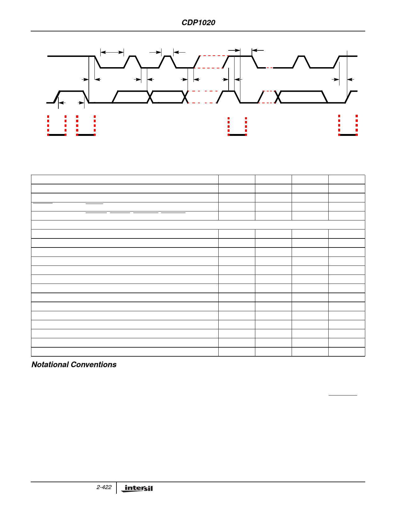
SCK
SDA
tLOW
tHD:STA
tBUF
tHIGH
tHD:DAT
tSU:DAT
tHD:STA
tSU:STA
tSU:STO
STOP
START
STOP
FIGURE 1. CONTROL TIMING
START
Control Timing VDD = 3.3V ±10%, TA = 0oC to 85oC
PARAMETER
Frequency Of Operation (4.0MHz nominal) (CLK Pin)
Suspend Recovery Start-up Time
RESET Pulse Width (RESET Pin)
Input Debounce Time (1394PRx, USBPRx, REMREQx, SECUREx Pins)
SMBus SCK and SDA Pins
SCK Frequency
SMBus Free Time
Hold Time After (Repeated) Start Condition
Repeated Start Condition Setup Time
Stop Condition Setup Time
Data Hold Time
Data Setup Time
SCK Time-out Period
SCK Low Period
SCK High Period
Slave SCK Extend Period (cumulative)
Master SCK Extend Period (cumulative)
SCK/SMBDAT Fall Time
SCK/SMBDAT Rise Time
Notational Conventions
The following conventions are used throughout this
document:
• Hexadecimal numbers are denoted with a “$” symbol
preceding the number.
• Binary numbers are represented with a “%” symbol
proceeding the number, or a “b” following.
• Because of the large mix of active-low and active-high
signals used in connection with the CDP1020, the terms
“asserted” and “de-asserted” will be used exclusively. An
active low signal is asserted when it is at a logic 0 and de-
asserted when it is at a logic 1 state. Conversely, an active
high signal is at a logic 1 state when asserted and at a
logic 0 state when de-asserted. The terms reset, clear,
SYMBOL
MIN
fCLK
2.0
tRSUS
0.9
tRL
6
tDB
50
fSMB
10
tBUF
4.7
tHD:STA
4.0
tSU:STA
4.7
tSU:STO
4.0
tHD:DAT
300
tSU:DAT
250
tTIMEOUT
25
tLOW
4.7
tHIGH
4.0
tLOW:SEXT
-
tLOW:MEXT
-
tF
-
tR
-
MAX
4.5
1
-
-
100
-
-
-
-
-
-
35
-
50
25
10
300
1000
UNITS
MHz
ms
tOSC
ms
kHz
µs
µs
µs
µs
ns
ns
ms
µs
µs
ms
ms
ns
ns
and “low” can also mean logic 0; set or “high” can also
mean logic 1.
• Active low signals are represented with an overline; active
high signals have no overline. For example, REMREQ0 is
active low, PWREN0 is active high.
• There are many pins, signals, registers, and software bits
common to both Bay 0 and Bay 1; these names may
include the Bay number suffix (0 or 1), an “x” to represent
either, or no suffix at all. For example, PWREN, PWREN0,
or PWRENx may each be used to describe output pin(s).
2-422
Share Link: 