RF2689 Ver la hoja de datos (PDF) - RF Micro Devices
Número de pieza
componentes Descripción
Lista de partido
RF2689 Datasheet PDF : 20 Pages
| |||
RF2689
Preliminary
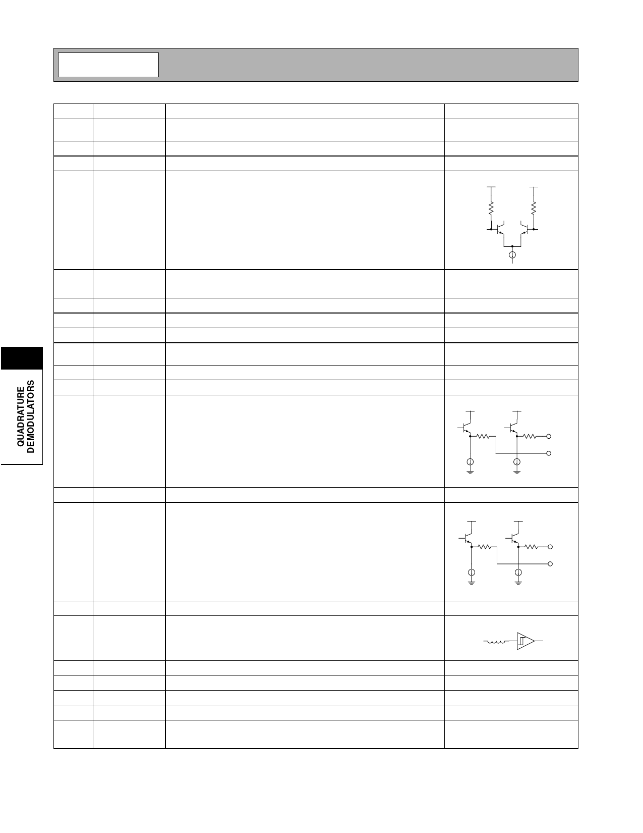
Pin Function Description
Interface Schematic
1
VGC1
Analog gain control. Valid control voltage ranges are form 0.5V to 2.5V.
These voltages are valid with a 10kΩ resistor in series with GC pin.
2
GSM IN+ GSM IF balanced input. Input internally DC-biased.
3
GSM IN- Same as pin 2.
4
W-CDMA W-CDMA IF balanced input. Input internally DC-biased.
IN+
BIAS
BIAS
1200 Ω
1200 Ω
W-CDMA IN+
W-CDMA IN-
5
W-CDMA Same as pin 4.
See pin 4.
IN-
6
VCC
Supply
7
MODE A DCS/GSM/GSM RX/W-CDMA mode selection.
8
LO
LO input pin. Input internally DC-biased.
7
9
MODE B Warm-up mode enable. The input LO buffers and divider chains are
enabled.
10
EN RX
Chip enable.
11
Q OUT- Complementary output to Q OUT+.
12
Q OUT+ Balanced baseband output.
VCC
VCC
150 µA
150 µA
Q OUT+
Q OUT-
13
I OUT-
Complementary output to I OUT+.
14
I OUT+ Balanced baseband output.
VCC
VCC
150 µA
150 µA
I OUT+
I OUT-
15
CALEN Calibration enable.
16
FCLK
FCLK clock reference for the automatic calibration circuitry.
20 kΩ
17
18
19
20
Pkg
Base
IF-
IF+
VREF2V
VGC2
Die
Flag
Complementary output to IF+.
IF test point output.
2V voltage reference decouple.
Gain control decouple.
Ground.
7-44
Rev A4 010815
Share Link: 