M5295AL Ver la hoja de datos (PDF) - MITSUBISHI ELECTRIC
Número de pieza
componentes Descripción
Lista de partido
M5295AL Datasheet PDF : 8 Pages
| |||
MITSUBISHI<Dig.Ana.INTERFACE>
M5295AL/P/FP
WATCHDOG TIMER
TERMINOLOGY
tRST1:Time required for TC pin potential to rise
from 0V VTH3(L) when Vcc is being applied.
tWD: Time required for TC pin potential to rise
from VTH3(L) to VTH3(H).
tRST2:Time required for TC pin potential to go
down from VTH3(H) to VTH3(L).
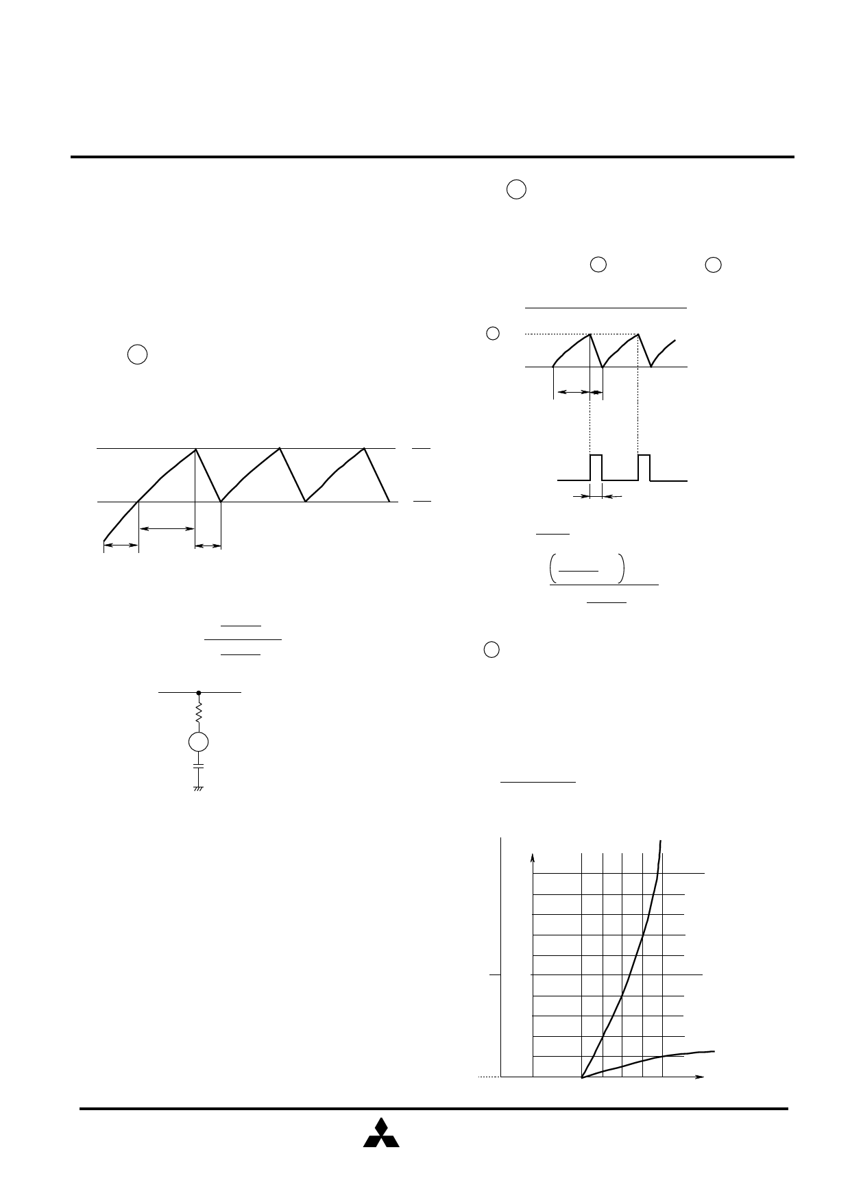
1.Pin 2 (TC Pin) Charge Time and
Discharge Time
When input to WD pin is abnormal,TC pin output
waveform is as shown below:
TC
0V
tWD
tRST(1)
tRST(2)
tRST(1)=0.51•C•R1
tWD=1.1•C•R1(charge time)
4• R1 -1
tRST(2)=1000•C•in 1000
2• R1
1000
-3
(discharge time)
Vcc
R1
2
C
Resistance R1:10kΩ≤R1≤30kΩ
When R1 is 10kΩ,tRST(2) is 830•C.
2.Pin 1 (WD Pin) Input Frequency,
Input Pulse Width,Charge Time and
Discharge Time
When input to WD pin 1 is normal,TC pin 2 output
waveform is as shown below:
(Vcc=5V)
4V
Pin 2 xV
2V
t1 t2
4
5 •Vcc
Input
2
5 •Vcc
tWDIN
t1=C•R1•in
3
5-x
(charge time)
t2=1000•C•in
R1
1000
+1
x-5
2• R1 -3
1000
(discharge time)
PIN 1 (WD PIN)INPUT REQUIREMENTS
(1)Connect capacitor between WD pin and voltage input.
(Refer to Section 3.)
(2)Input cycle:No more than tWD
(Discharge should start before voltage at WD pin
reaches 4V.)
1
<f
1.1•C•R1
(3)Input pulse width tWDIN:No more than t2
C=104
1ms t
C=103
100µs
t1
Vcc=5V
50µs 0.5
ms
R1=10kΩ
MITSUBISHI
ELECTRIC
t2
234
DISCHARGE VOLTAGE x(V)
( 4/8 )
Share Link: 