LPC47U327 Ver la hoja de datos (PDF) - SMSC -> Microchip
Número de pieza
componentes Descripción
Lista de partido
LPC47U327
SMSC -> Microchip

LPC47U327 Datasheet PDF : 252 Pages
| |||
DESCRIPTION OF PIN FUNCTIONS
The pins that have multiple functions are named
with the primary function first. The primary
function is the function of the pin at default. For
example, GP40/DRVDEN0 pin has the primary
function of GP40.
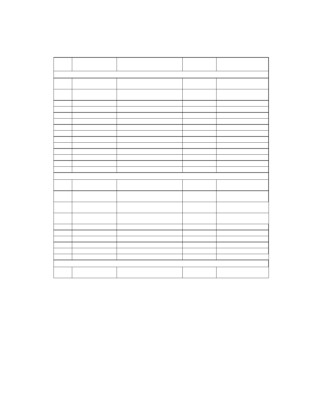
QFP
PIN #
60
61
62
63
64
65
66
67
68
69
70
71
72
73
21
22
23
24
25
26
27
28
30
31
2
NAME
GP40/DRVDEN0
GP41/DRVDEN1
nMTR0
nDSKCHG
nDS0
nDIR
nSTEP
nWDATA
nWGATE
nHDSEL
nINDEX
nTRK0
nWRTPRT
nRDATA
LAD0
LAD1
LAD2
LAD3
nLFRAME
nLDRQ
nPCI_RESET
nLPCPD
PCI_CLK
SER_IRQ
GP10/J1B1
TABLE 1 - PIN FUNCTION DESCRIPTION
FUNCTION
BUFFER
TYPE
FDD INTERFACE
General Purpose I/O/Drive
Density Select 0
General Purpose I/O/Drive
Density Select 1
Motor On 0
Disk Change
Drive Select 0
Step Direction
Step Pulse
Write Disk Data
Write Gate
Head Select
Index Pulse Input
Track 0
Write Protected
Read Disk Data
IO12
IO12
O12
IS
O12
O12
O12
O12
O12
O12
IS
IS
IS
IS
LPC INTERFACE
Multiplexed Command
Address and Data 0
Multiplexed Command
Address and Data 1
Multiplexed Command
Address and Data 2
Multiplexed Command
Address and Data 3
Frame
Encoded DMA Request
PCI Reset
Power Down (Note 2)
PCI Clock
Serial IRQ
PCI_IO
PCI_IO
PCI_IO
PCI_IO
PCI_I
PCI_O
PCI_I
PCI_I
PCI_ICLK
PCI_IO
GAME PORT INTERFACE
General Purpose
I/O/Joystick 1 Button 1
IS/O8
BUFFER MODE PER
FUNCTION (NOTE 1)
IO12/(O12/OD12)
IO12/(O12/OD12)
(O12/OD12)
IS
(O12/OD12)
(O12/OD12)
(O12/OD12)
(O12/OD12)
(O12/OD12)
(O12/OD12)
IS
IS
IS
IS
PCI_IO
PCI_IO
PCI_IO
PCI_IO
PCI_I
PCI_O
PCI_I
PCI_I
PCI_ICLK
PCI_IO
(IS/O8/OD8)/IS
7
Share Link: