COM20022I Ver la hoja de datos (PDF) - SMSC -> Microchip
Número de pieza
componentes Descripción
Lista de partido
COM20022I Datasheet PDF : 88 Pages
| |||
Selection of 8/16-Bit Access
The interface to the internal RAM is software
selectable as either 8 or 16-bit. This feature is
new to the COM20022. The D15-D8 pins are the
upper-byte data bus pins. The nIOCS16 pin is the
16-bit I/O access enable output pin. This pin is
active low for a 16-bit RAM access by the CPU
(not a DMA access).
The 16-bit access mode is enabled and disabled
through the W16 bit located in the Bus Control
Register at bit 7. The SWAP bit is used to swap
the upper and lower data bytes in 16-bit mode,
as shown in the table below. The SWAP bit is
located at bit 0 of Address Low Pointer. This
location is same as the A0 bit; when 16 bit
access is enabled (W16 =1), the A0 bit becomes
the SWAP bit.
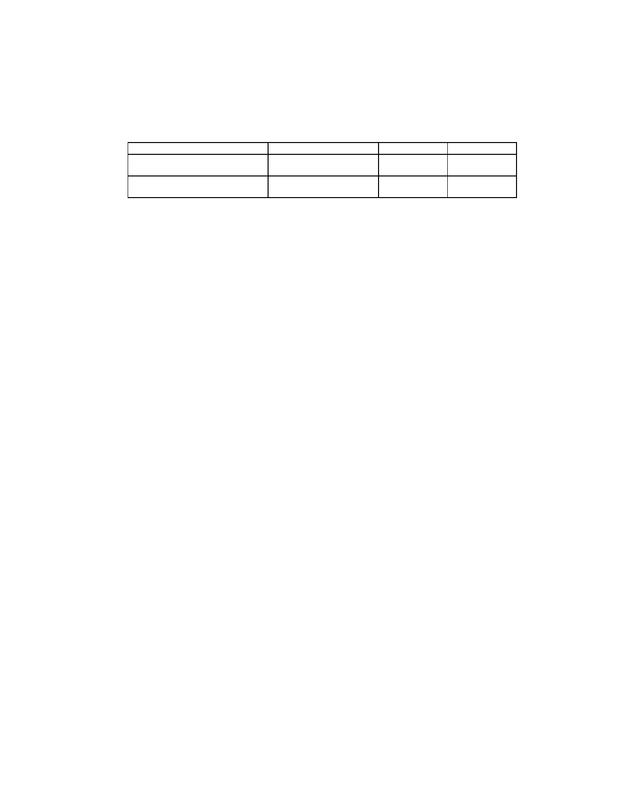
DETECTED HOST I/F MODE
SWAP BIT (NOTE) D15-D8 PINS
Intel 80xx Mode
0
Odd
(RD,WR Mode)
1
Even
Motorola 68xx Mode
0
Even
(DIR, DS Mode)
1
Odd
Note: The SWAP bit is undefined after a hardware reset
D7-D0 PINS
Even
Odd
Odd
Even
As shown on the table above, even address data The DMA interface consists of several added
is to/from D7-D0 pins and odd address data is pins. The DREQ pin is the DMA Request output
to/from D15-D8 pins when detected host pin. The active polarity of this pin is
interface mode is Intel 80xx mode and the programmable; the default is active-high. The
SWAP bit is not set. The odd address data is nDACK pin is the active-low DMA acknowlege
to/from the D7-D0 pins and the even address input pin. The TC pin is the external terminal
data is to/from D15-D8 pins when detected host count input pin. This pin determines when the
interface mode is Motorola 68xx mode and the nDACK pin is active. It’s active polarity is
SWAP bit is not set.
programmable; the default is active-high. The
nREFEX pin is the active-low refresh execution
When disabling 16-bit access, the D15-D8 pins pulse input pin.
are always Hi-Z. The D15-D8 pins are Hi-Z when
enabling 16-bit access except for internal RAM The DMA interface is controlled by the following
access.
bits. The DMAEND bit selects whether or not to
mask the interrupt upon finishing the DMA. This
W16 bit and SWAP bit influence both the CPU bit is located at bit 4 of the Mask register. The
cycle and DMA cycle.
DMAEN bit is used to disable/enable the
assertion of the DMA Request (DREQ pin) after
DMA Transfers To And From Internal RAM
writing the Address Pointer Low register. This bit
is located in the Address Pointer High register,
The COM20022 supports DMA transfers to and
from the internal RAM. This feature is new to the
COM20022. The software selectable 8/16 bit
interface to the RAM pertains to DMA transfers.
When the W16 bit=0, the microcontroller
interface and DMA transfers are both 8-bit data
bit 3. The following bits are located in the Bus
Control Register: DRPOL, TCPOL and
DMAMD[1,0]. The DRQPOL bit sets the active
polarity of the DREQ pin; the TCPOL bit sets the
active polarity of the TC pin; the DMAMD[1,0]
bits select the data transfer mode of the DMA.
transfers to/from internal RAM. When W16=1
they are both 16-bit data transfers. An 8-bit
microcontroller interface and 16-bit DMA data
transfer cannot be selected; they must be the
same width data transfers to/from internal RAM.
The ITCEN/RTRG bit has one of two functions,
depending on the DMA transfer mode selected.
ITCEN is the Internal Terminal Counter Enable.
It is used to select whether the DMA is
terminated by external TC only or by either
The data swapping operation on 16-bit data
transfers also pertains to both.
internal or external TC. ITCEN is for Non-Burst
or Burst mode. RTRG selects the re-trigger
17
Share Link: 