CAM35C44 Ver la hoja de datos (PDF) - SMSC -> Microchip
Número de pieza
componentes Descripción
Lista de partido
CAM35C44 Datasheet PDF : 50 Pages
| |||
Multiplexed Addressing
When multiplexed address modes are selected,
i.e. HS[1:0] = 02H or 03H (TABLE 3), register
addresses are decoded from the Multiplexed
Address/Data Bus AD[7:0], the Block Select bits
BS[2:0] and the chip select nCS pin.
In the multiplexed addressing modes the 5 low-
order bits of the Multiplexed Address/Data Bus
AD[4:0] determine the register address while the
Block Select bits BS[2:0] qualify the
three high-order Multiplexed Address/Data Bus
bits, AD[7:5]; i.e., BS[2:0] decodes which of eight
32-byte blocks is selected in the 256-byte page
decoded by nCS. Note: page address decoding
must be done externally.
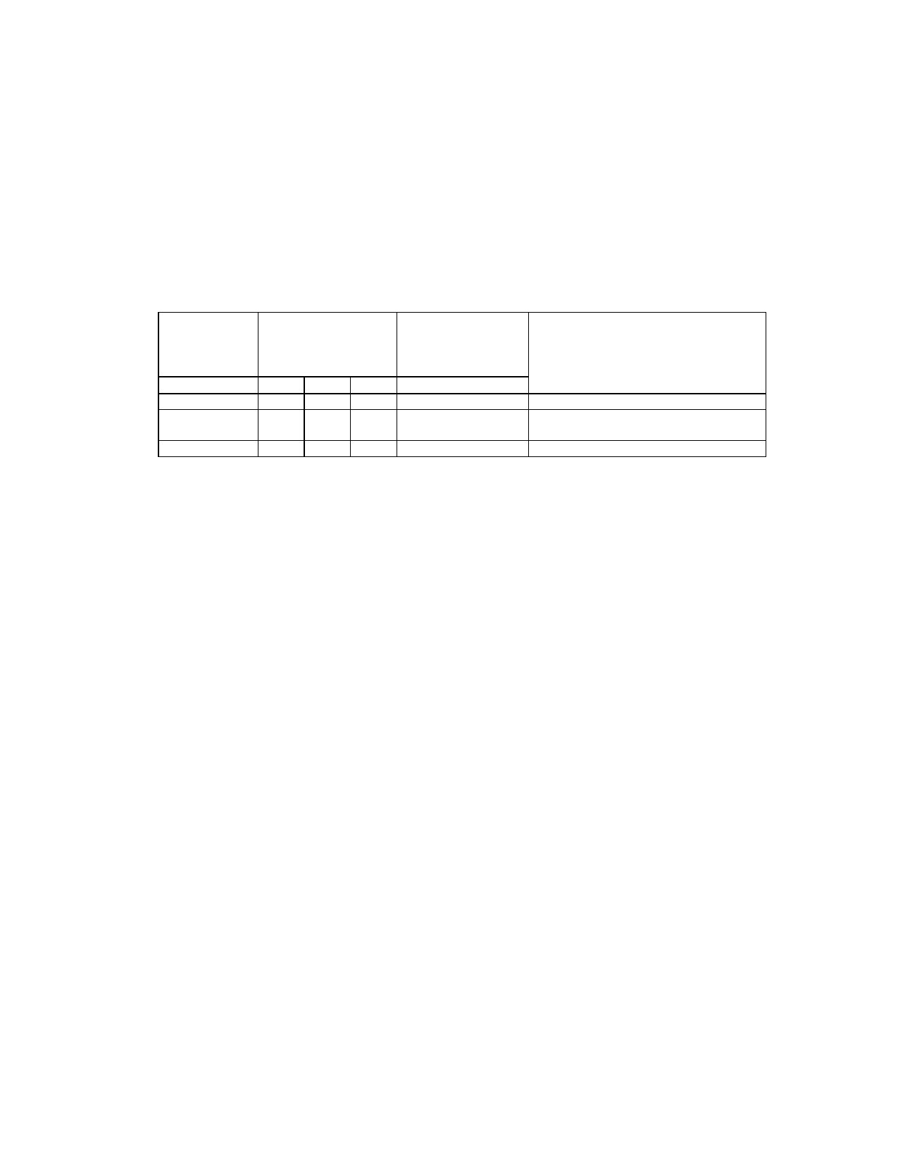
For example, TABLE 10 illustrates that if BS[2:0]
= 01H, nCS = 0 (active), and AD[7:0] = 20H, the
Index Register in the Configuration Bank has
been selected.
Two extra GPIO pins GPIO[4:3] are available in
the multiplexed address modes.
TABLE 10 - EXAMPLE MULTIPLEXED ADDRESS DECODING
256-BYTE
ADDRESS
PAGE
nCS
1
0
0
32-BYTE ADDRESS
BLOCK
BS2 BS1 BS0
0
0
1
0
0
1
0
0
1
MULTIPLEX
ADDR/DATA BUS
AD[7:0]
XXH
20H
00H
DESCRIPTION
No Decode: Invalid Page
Decode Configuration Bank Index
Register (TABLE 12)
No Decode: Invalid Block
17
Share Link: 