CAM35C44 Ver la hoja de datos (PDF) - SMSC -> Microchip
Número de pieza
componentes Descripción
Lista de partido
CAM35C44 Datasheet PDF : 50 Pages
| |||

Configuration Registers
Introduction
Configuration Register references are in hex;
e.g., CRC0.3 means Configuration Register
0xC0, Bit 0x03.
The configuration registers (TABLE 13) are set
to their default values at power up and are not
affected by RESET, except where noted in the
register descriptions that follow.
Configuration register bits that are not needed in
the CAM35C44 are marked RESERVED in the
sections below. RESERVED bits cannot be
written and return “0” when read.
Configuration Bank Addressing
The CONFIGURATION register bank is defined
as the first eight addresses in the CAM35C44
memory map (see section REGISTER
ADDRESS MAP on page 16).
TABLE 12 summarizes the contents of the
CONFIGURATION bank. The Index and Data
registers access the configuration registers
(TABLE 13) as described above.
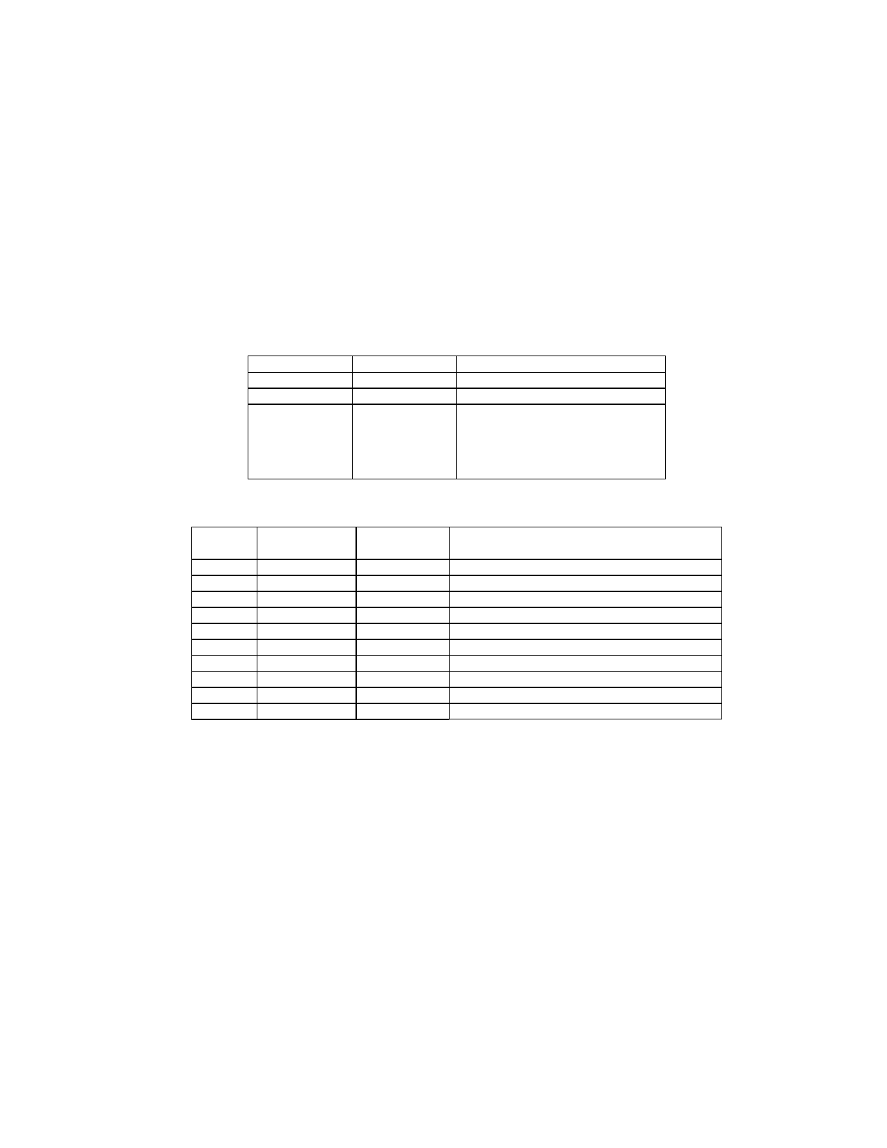
TABLE 12 - CONFIGURATION REGISTER BANK
ADDRESS
DEFAULT
REGISTER NAME
0x00
0x00
Config/Index Register
0x01
0x00
Data Register
0x02
0x00
RESERVED
.
.
.
0x07
Description
CR
INDEX
0x00
0x01
0x02
0x03
0x04
0x05
0x06
0x07
0x08
0x09
TABLE 13 - CONFIGURATION REGISTERS
POR
RESET
DEFAULT
DEFAULT
REGISTER NAME
0x00
0x00
IRQ CONTROL
0x00
0x00
DMA CONTROL
0x02
n/a
INFRARED OPTION
0x01
n/a
INFRARED CONTROL B
0x00
n/a
TEST CONTROL A
0x00
n/a
SOFTWARE SELECT A
0x00
n/a
SOFTWARE SELECT B
0x03
n/a
IR HALF DUPLEX TIME-OUT
0x00
0x00
POWER CONTROL
0x00
n/a
TEST CONTROL B
21