5962R9571401QRC(1996) Ver la hoja de datos (PDF) - Intersil
Número de pieza
componentes Descripción
Lista de partido
5962R9571401QRC Datasheet PDF : 6 Pages
| |||
Specifications HS-82C08RH
Absolute Maximum Ratings
Reliability Information
Supply Voltage . . . . . . . . . . . . . . . . . . . . . . . . . . . . . . . . . . . . . +7.0V
Input, Output or I/O Voltage . . . . . . . . . . . . GND-0.3V to VDD+0.3V
Storage Temperature Range . . . . . . . . . . . . . . . . . -65oC to +150oC
Junction Temperature . . . . . . . . . . . . . . . . . . . . . . . . . . . . . . +175oC
Lead Temperature (Soldering 10s) . . . . . . . . . . . . . . . . . . . . +300oC
ESD Classification . . . . . . . . . . . . . . . . . . . . . . . . . . . . . . . . Class 1
Thermal Resistance
θJA
θJC
20 Lead SBDIP Package. . . . . . . . . . . . . 71oC/W 17oC/W
20 Lead Ceramic Flatpack Package . . . . 85oC/W 25oC/W
Maximum Package Power Dissipation at +125oC Ambient
20 Lead SBDIP Package. . . . . . . . . . . . . . . . . . . . . . . . . . . 0.70W
20 Lead Ceramic Flatpack Package . . . . . . . . . . . . . . . . . . 0.59W
If device power exceeds package dissipation capability, provide heat
sinking or derate linearly at the following rate:
20 Lead SBDIP Package. . . . . . . . . . . . . . . . . . . . . . . .14.1mW/C
20 Lead Ceramic Flatpack Package . . . . . . . . . . . . . . . 11.8mW/C
CAUTION: Stresses above those listed in “Absolute Maximum Ratings” may cause permanent damage to the device. This is a stress only rating and operation
of the device at these or any other conditions above those indicated in the operational sections of this specification is not implied.
Operating Conditions
Operating Voltage Range . . . . . . . . . . . . . . . . . . . +4.75V to +5.25V
Operating Temperature Range . . . . . . . . . . . . . . . . -55oC to +125oC
Input Low Voltage . . . . . . . . . . . . . . . . . . . . . . . . . . . . . . . 0V to +1V
Input High Voltage. . . . . . . . . . . . . . . . . . . . . . . . . . VDD -1V to VDD
TABLE 1. DC ELECTRICAL PERFORMANCE CHARACTERISTICS
All Devices Guaranteed at Worst Case Limits and Conditions.
PARAMETER
Input Leakage Current
High Level Output
Voltage
Low Level Output
Voltage
Static Current
Functional Test
SYMBOL
CONDITIONS
GROUP A
SUBGROUPS
IIL
VDD = 5.25V, VIN = VDD
Pin Under Test = 0V
1, 2, 3
IIH
VDD = 5.25V, VIN = 0V
Pin Under Test = 5.25V
1, 2, 3
VOH VDD = 4.75V, IOH = -2.0mA
1, 2, 3
VOL VDD = 5.25V, IOL = 2.0mA
1, 2, 3
SIDD VDD = 5.25V, VIN = GND
1, 2, 3
FT
VDD = 4.75V to 5.25V
7, 8A, 8B
VIH = VDD -1.0V, VIL = 1.0V
TEMPERATURE
-55oC, +25oC,
+125oC
-55oC, +25oC,
+125oC
-55oC, +25oC,
+125oC
-55oC, +25oC,
+125oC
-55oC, +25oC,
+125oC
-55oC, +25oC,
+125oC
LIMITS
MIN MAX
-1.0
-
UNITS
µA
-
1.0
µA
4.25
-
V
-
0.5
V
-
100
µA
-
-
-
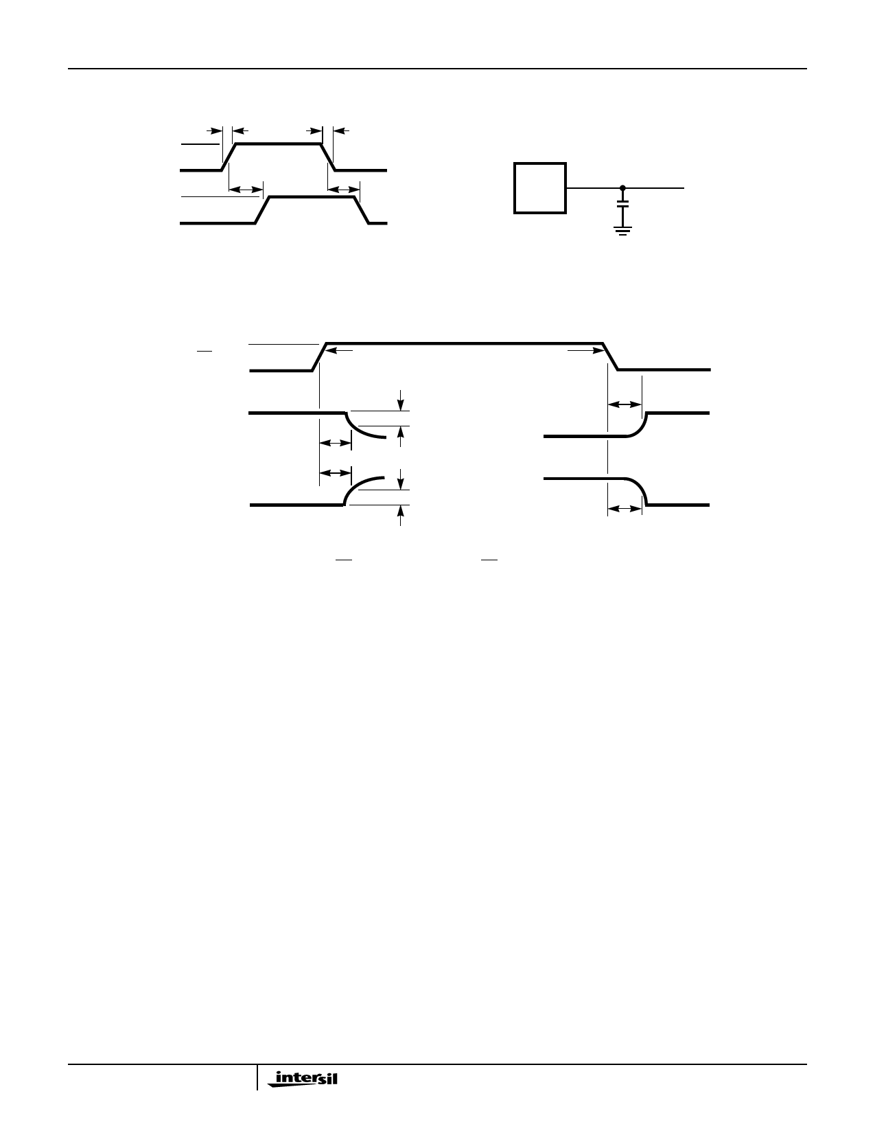
TABLE 2. AC ELECTRICAL PERFORMANCE CHARACTERISTICS
PARAMETER
PORT DATA/MODE SPECIFICATIONS
Propagation Delay to Logical “1” from Port
A, B to Port B, A
Propagation Delay to Logical “0” from Port
A, B to Port B, A
Propagation Delay from High-Impedance
to Logical “1” from T/R to Port
Propagation Delay from High-Impedance
to Logical “0” from T/R to Port
Propagation Delay from High-Impedance
to Logical “1” from OE to Port
Propagation Delay from High-Impedance
to Logical “0” from OE to Port
SYMBOL
TPDLH
TPDHL
TPRTH
TPRTL
TPZH
TPZL
GROUP A
SUBGROUPS
9, 10, 11
9, 10, 11
9, 10, 11
9, 10, 11
9, 10, 11
9, 10, 11
TEMPERATURE
-55oC, +25oC, +125oC
-55oC, +25oC, +125oC
-55oC, +25oC, +125oC
-55oC, +25oC, +125oC
-55oC, +25oC, +125oC
-55oC, +25oC, +125oC
LIMITS
MIN MAX
-
65
-
80
-
75
-
130
-
70
-
130
UNITS
ns
ns
ns
ns
ns
ns
Spec Number 518057
3
Share Link: 