HFBR-5103A Ver la hoja de datos (PDF) - HP => Agilent Technologies
Número de pieza
componentes Descripción
Lista de partido
HFBR-5103A
HP => Agilent Technologies

HFBR-5103A Datasheet PDF : 21 Pages
| |||
Solder and Wash Process
Compatibility
The transceivers are delivered
with protective process plugs
inserted into the duplex SC or
duplex ST connector receptacle.
This process plug protects the
optical subassemblies during
wave solder and aqueous wash
processing and acts as a dust
cover during shipping.
Board Layout - Mechanical
For applications providing a
choice of either a duplex SC or a
duplex ST connector interface,
while utilizing the same pinout on
the printed circuit board, the ST
port needs to protrude from the
chassis panel a minimum of
9.53 mm for sufficient clearance
to install the ST connector.
;; These transceivers are compatible
with either industry standard
wave or hand solder processes.
Shipping Container
The transceiver is packaged in a
shipping container designed to
protect it from mechanical and
ESD damage during shipment or
Rx
storage.
NO INTERNAL CONNECTION
Please refer to Figure 8A for a
mechanical layout detailing the
recommended location of the
duplex SC and duplex ST
transceiver packages in relation to
the chassis panel.
For both shielded design options,
Figure 8b identifies front panel
aperture dimensions.
;;Tx
NO INTERNAL CONNECTION
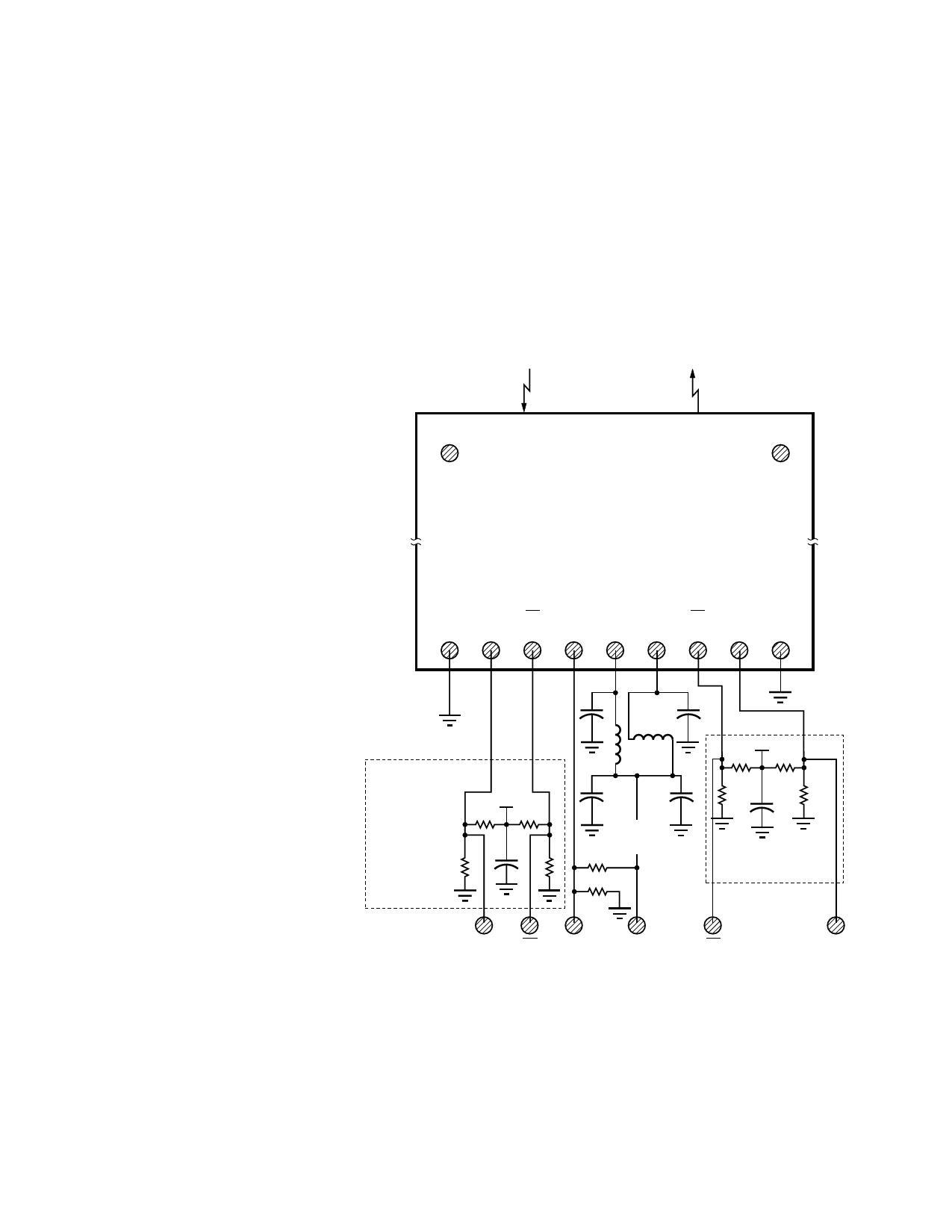
Board Layout - Decoupling Circuit
and Ground Planes
It is important to take care in the
layout of your circuit board to
achieve optimum performance
from these transceivers. Figure 7
provides a good example of a
schematic for a power supply
decoupling circuit that works well
with these parts. It is further
recommended that a contiguous
ground plane be provided in the
circuit board directly under the
transceiver to provide a low
inductance ground for signal
return current. This
recommendation is in keeping
with good high frequency board
layout practices.
Board Layout - Hole Pattern
The Agilent transceiver complies
with the circuit board “Common
Transceiver Footprint” hole
pattern defined in the original
multisource announcement which
defined the 1x9 package style.
This drawing is reproduced in
Figure 8 with the addition of ANSI
Y14.5M compliant dimensioning
to be used as a guide in the
mechanical layout of your circuit
board.
;;;;;HFBR-510X
TOP VIEW
Rx
Rx Tx
Tx
VEE RD RD SD VCC VCC TD TD VEE
1
2
3
4
5
6
7
8
9
C1
C2
VCC
TERMINATION
L1 L2
R2 R3
;;;;;; AT PHY
DEVICE
INPUTS
VCC
R5
R7
C6
R6
R8
C3
C4
VCC FILTER
AT VCC PINS
TRANSCEIVER
R9
R10
R1
R4
C5
TERMINATION
AT TRANSCEIVER
INPUTS
RD RD SD
VCC
TD
TD
NOTES:
THE SPLIT-LOAD TERMINATIONS FOR ECL SIGNALS NEED TO BE LOCATED AT THE INPUT
OF DEVICES RECEIVING THOSE ECL SIGNALS. RECOMMEND 4-LAYER PRINTED CIRCUIT
BOARD WITH 50 OHM MICROSTRIP SIGNAL PATHS BE USED.
R1 = R4 = R6 = R8 = R10 = 130 OHMS.
R2 = R3 = R5 = R7 = R9 = 82 OHMS.
C1 = C2 = C3 = C5 = C6 = 0.1 µF.
C4 = 10 µF.
L1 = L2 = 1 µH COIL OR FERRITE INDUCTOR.
Figure 7. Recommended Decoupling and Termination Circuits
8
Share Link: