HM-6551/883 Ver la hoja de datos (PDF) - Intersil
Número de pieza
componentes Descripción
Lista de partido
HM-6551/883 Datasheet PDF : 10 Pages
| |||
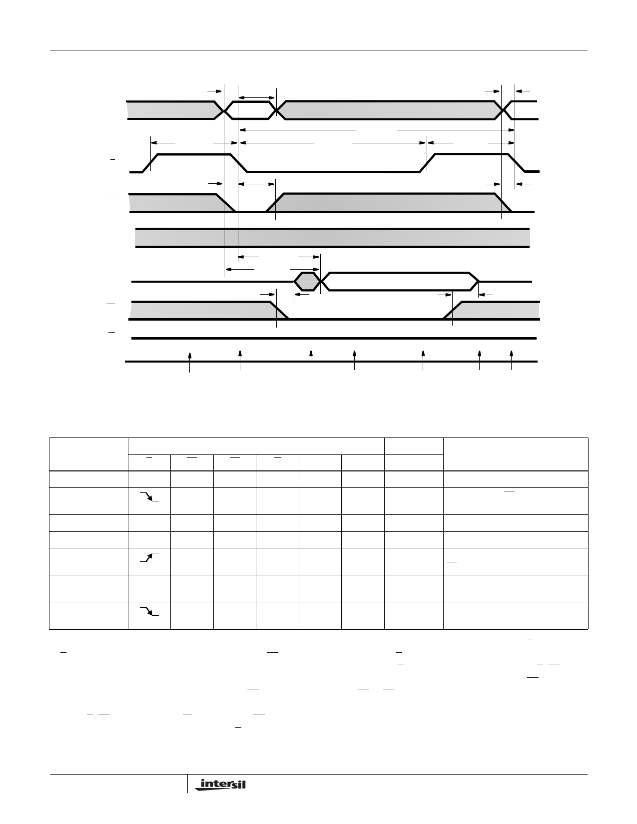
Timing Waveforms
(8) TAVEL
A
(7) TEHEL
E
(9) TS2LEL
S2
HM-6551/883
(10)
TELAX
VALID
TELS2X
(11)
(19) TELEL
TELEH (6)
(8) TAVEL
NEXT
TEHEL (7)
(9) TS2LEL
D
Q
S1
W
TIME
REFERENCE
HIGH
TELQV (1)
TAVQV (2)
(3) TS1LQX
VALID OUTPUT
-1
0
1
2
3
FIGURE 1. READ CYCLE
TS1HQZ (5)
4
5
TIME
REFERENCE
E
-1
H
0
1
L
2
L
3
4
H
5
TRUTH TABLE
INPUTS
OUTPUTS
S1
S2
W
A
D
Q
FUNCTION
H
X
X
X
X
Z
Memory Disabled
X
L
H
V
X
Z
Addresses and S2 are Latched,
Cycle Begins
L
X
H
X
X
X
Output Enabled but Undefined
L
X
H
X
X
V
Data Output Valid
L
X
H
X
X
V
Outputs Latched, Valid Data,
S2 Unlatches
H
X
X
X
X
Z
Prepare for Next Cycle
(Same as -1)
X
L
H
V
X
Z
Cycle Ends, Next Cycle Begins
(Same as 0)
The HM-6551/883 Read Cycle is initiated by the falling edge
of E. This signal latches the input address word and S2 into
on-chip registers providing the minimum setup and hold
times are met. After the required hold time, these inputs may
change state without affecting device operation. S2 acts as a
high order address and simplifies decoding. For the output to
be read, E, S1 must be low and W must be high. S2 must
have been latched low on the falling edge of E. The output
data will be valid at access time (TELQV). The HM-6551/883
has output data latches that are controlled by E. On the
rising edge of E the present data is latched and remains in
that state until E falls. Also on the rising edge of E, S2
unlatches and controls the outputs along with S1. Either or
both S1 or S2 may be used to force the output buffers into a
high impedance state.
6
Share Link: 