LTC1150M(RevB) Ver la hoja de datos (PDF) - Linear Technology
Número de pieza
componentes Descripción
Lista de partido
LTC1150M Datasheet PDF : 16 Pages
| |||
LTC1150
APPLICATIO S I FOR ATIO
Table 1. Resistor Thermal EMF
RESISTOR TYPE
Tin Oxide
Carbon Composition
Metal Film
WireWound
Evenohm
Manganin
THERMAL EMF/°C GRADIENT
~mV/°C
~450µV/°C
~20µV/°C
~2µV/°C
~2µV/°C
PACKAGE-INDUCED OFFSET VOLTAGE
Package-induced thermal EMF effects are another impor-
tant source of errors. It arises at the copper/kovar
junctions formed when wire or printed circuit traces
contact a package lead. Like all the previously mentioned
thermal EMF effects, it is outside the LTC1150’s offset
nulling loop and cannot be cancelled. Metal can
H packages exhibit the worst warm-up drift. The input
offset voltage specification of the LTC1150 is actually set
by the package-induced warm-up drift rather than by the
circuit itself. The thermal time constant ranges from 0.5 to
3 minutes, depending on package type.
ALIASING
Like all sampled data systems, the LTC1150 exhibits
aliasing behavior at input frequencies near the sampling
frequency. The LTC1150 includes a high-frequency
correction loop which minimizes this effect; as a result,
aliasing is not a problem for most applications.
For a complete discussion of the correction circuitry and
aliasing behavior, please refer to the LTC1051/53 data
sheet.
SYNCHRONIZATION OF MULTIPLE LTC115O’S
When synchronization of several LTC1150’s is required,
one of the LTC1150’s can be used to provide the “master”
clock to control over 100 “slave” LTC1150’s. The master
clock, coming from Pin 8 of the master LTC1150, can
directly drive Pin 5 of the slaves. Note that Pin 8 of the slave
LTC1150’s will be pulled up to VS.
If all the LTC1150’s are to be synchronized with an external
clock, then the external clock should drive Pin 5 of all the
LTC1150’s.
10
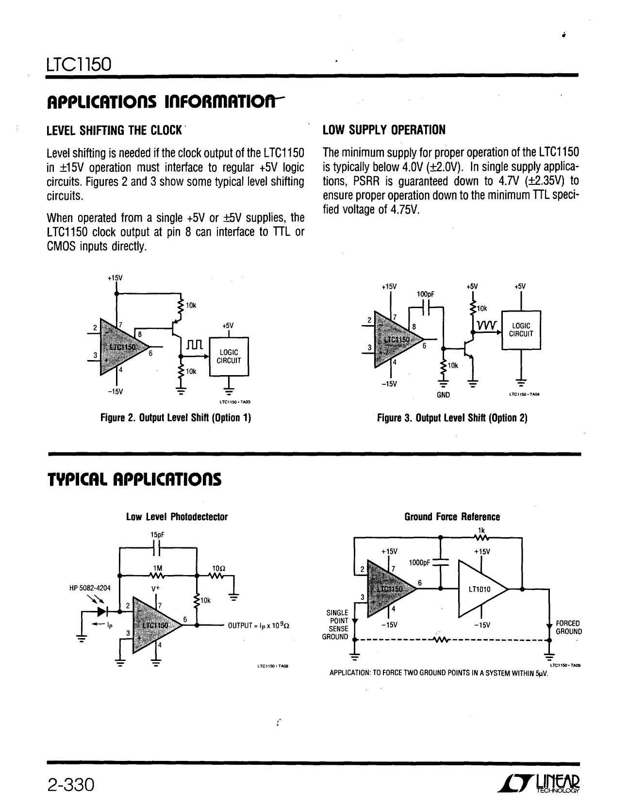
LEVEL SHIFTING THE CLOCK
Level shifting is needed if the clock output of the LTC1150
in ±15V operation must interface to regular 5V logic
circuits. Figures 2 and 3 show some typical level shifting
circuits.
When operated from single 5V or ±5V supplies, the
LTC1150 clock output at Pin 8 can interface to TTL or
CMOS inputs directly.
LOW SUPPLY OPERATION
The minimum supply for proper operation of the LTC1150
is typically below 4.0V (±2.0V). In single supply applica-
tions, PSRR is guaranteed down to 4.7V (±2.35V)
to ensure proper operation down to the minimum TTL
specified voltage of 4.75V.
15V
10k
2
7
8
LTC1150
6
3
4
5V
LOGIC
CIRCUIT
10k
–15V
LTC1150 • AI02
Figure 2. Output Level Shift (Option 1)
15V
100pF
2
7
8
6
LTC1150
3
4
5V
10k
10k
5V
LOGIC
CIRCUIT
–15V
GND
LTC1150 • AI03
Figure 3. Output Level Shift (Option 2)
1150fb
Share Link: 