LTC1150M(RevB) Ver la hoja de datos (PDF) - Linear Technology
Número de pieza
componentes Descripción
Lista de partido
LTC1150M Datasheet PDF : 16 Pages
| |||
FEATURES
■ High Voltage Operation: ±16V
■ No External Components Required
■ Maximum Offset Voltage: 10µV
■ Maximum Offset Voltage Drift: 0.05µV/°C
■ Low Noise 1.8µVP-P (0.1Hz to 10Hz)
■ Minimum Voltage Gain: 135dB
■ Minimum PSRR: 120dB
■ Minimum CMRR: 110dB
■ Low Supply Current: 0.8mA
■ Single Supply Operation: 4.75V to 32V
■ Input Common Mode Range Includes Ground
■ 200µA Supply Current with Pin 1 Grounded
■ Typical Overload Recovery Time 20ms
U
APPLICATIO S
■ Strain Gauge Amplifiers
■ Electronic Scales
■ Medical Instrumentation
■ Thermocouple Amplifiers
■ High Resolution Data Acquisition
LTC1150
±15V Zero-Drift
Operational Amplifier with
Internal Capacitors
DESCRIPTIO
The LTC®1150 is a high-voltage, high-performance
zero-drift operational amplifier. The two sample-and-hold
capacitors usually required externally by other chopper
amplifiers are integrated on-chip. Further, LTC’s propri-
etary high-voltage CMOS structures allow the LTC1150 to
operate at up to 32V total supply voltage.
The LTC1150 has an offset voltage of 0.5µV, drift of
0.01µV/°C, 0.1Hz to 10Hz input noise voltage of 1.8µVP-P
and a typical voltage gain of 180dB. The slew rate of 3V/µs
and a gain bandwidth product of 2.5MHz are achieved with
0.8mA of supply current. Overload recovery times from
positive and negative saturation conditions are 3ms and
20ms, respectively.
For applications demanding low power consumption,
Pin 1 can be used to program the supply current. Pin 5 is
an optional AC-coupled clock input, useful for
synchronization.
The LTC1150 is available in standard 8-lead, plastic dual-
in-line package, as well as an 8-lead SO package. The
LTC1150 can be a plug-in replacement for most standard
bipolar op amps with significant improvement in DC
performance.
, LTC and LT are registered trademarks of Linear Technology Corporation.
TYPICAL APPLICATIO
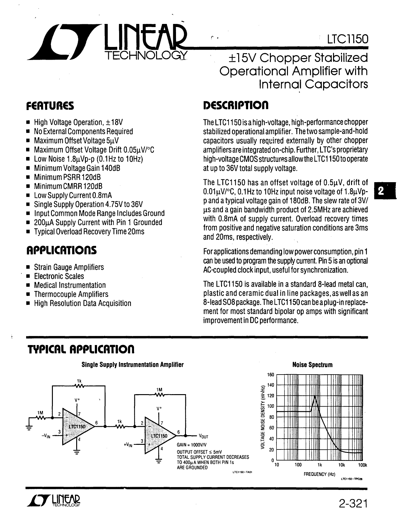
Single Supply Instrumentation Amplifier
1k
V+
1M
2
7
6
LTC1150
3
–VIN
4
1M
V+
1k
VIN
2
7
LTC1150
3
4
6
VOUT
GAIN = 1000V/V
OUTPUT OFFSET ≤ 5mV
TOTAL SUPPLY CURRENT
DECREASES TO 400µA
WHEN BOTH PIN 1s ARE
GROUNDED
LTC1150 •TA01
160
140
120
100
80
60
40
20
0
10
Noise Spectrum
100
1k
10k
100k
FREQUENCY (Hz)
LTC1150 •TA02
1150fb
1
Share Link: 