ST5R00 Ver la hoja de datos (PDF) - STMicroelectronics
Número de pieza
componentes Descripción
Lista de partido
ST5R00 Datasheet PDF : 15 Pages
| |||
ST5R00 SERIES
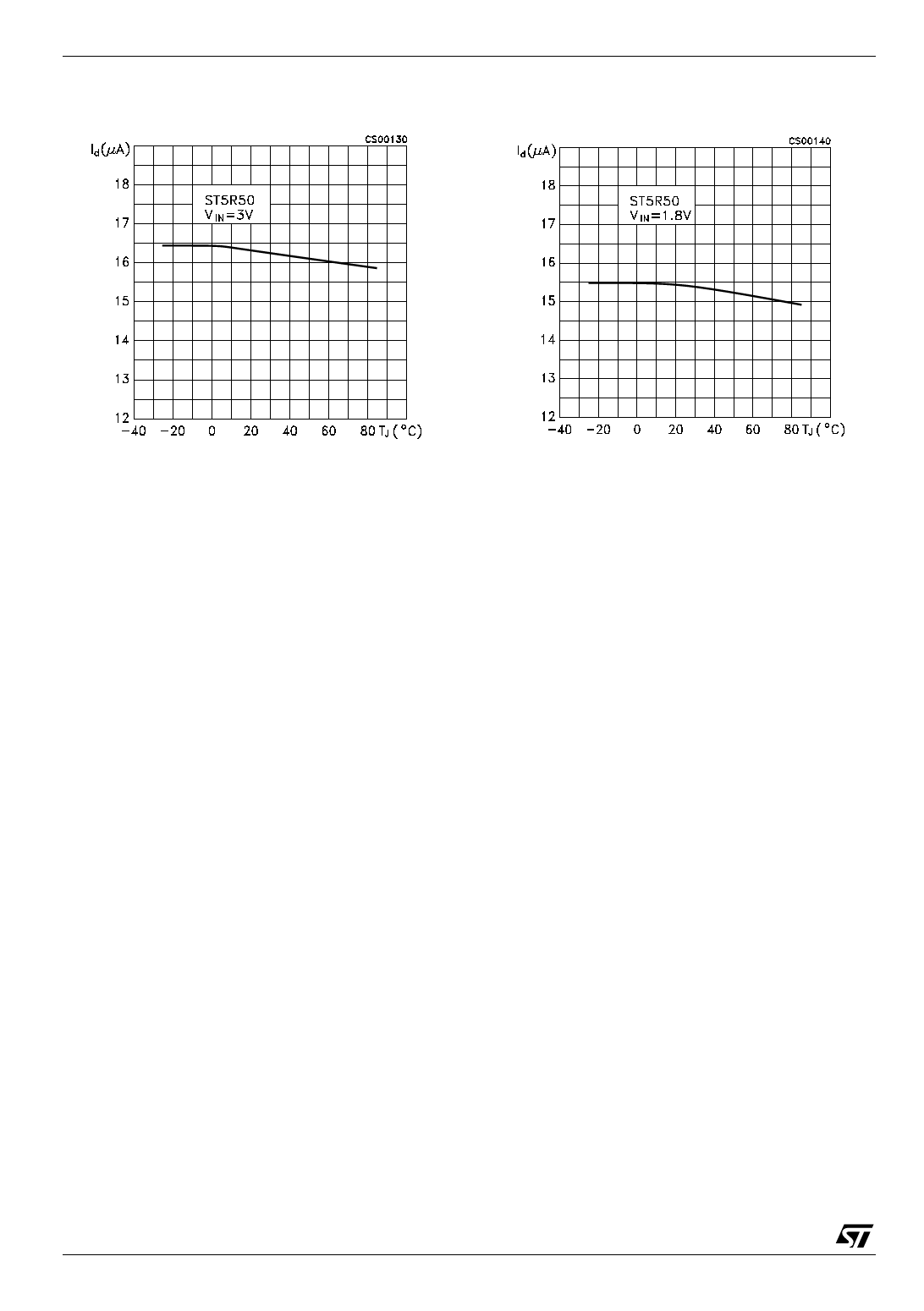
Figure 30: No Load Input Current vs
Temperature
Figure 31: No Load Input Current vs
Temperature
APPLICATION INFORMATION
PC LAYOUT AND GROUNDING HINTS
The ST5R00 high frequency operation makes PC layout important for minimizing ground bounce and
noise. Place external components as close as possible to the device pins. Take care to the Supply
Voltage Source connections that have to be very close to the Input of the application. Set the Output Load
as close as possible to the output capacitor. If possible, use a Star ground connection with the centre point
on the Device Ground pin. To maximize output power and efficiency and minimize output ripple voltage,
use a ground plane and solder the ICs ground pin directly to the ground plane.
Remember that the LX Switching Current flows through the Ground pin, so, in order to minimize the series
resistance that may cause power dissipation and decrease of the Efficiency conversion, the Ground
pattern has to be as large as possible.
INDUCTOR SELECTION
An inductor value of 47µH performs well in most ST5R00 applications. However, the inductance value is
not critical, and the ST5R00 will work with inductors in the 33µH to 120µH. Smaller inductance values
typically offer a smaller physical size for a given series resistance, allowing the smallest overall circuit
dimensions. However, due to higher peak inductor currents, the output voltage ripple (Ipeak x output filter
capacitors ESR) also tends to be higher. Circuits using larger inductance values exhibit higher output
current capability and larger physical dimensions for a given series resistance.
In order to obtain the best application performances the inductor must respect the following condition:
- The DC resistance has to be as little as possible, a good value is <0.25Ω. This choice will reduce the lost
power as heat in the windings.
- The inductor core must not saturate at the forecast maximum LX current. This is mainly a function of the
Input Voltage, Inductor value and Output Current. However, it is generally acceptable to bias the inductor
into saturation by as much as 20%, although this will slightly reduce efficiency. In order to calculate this
parameter we have to distinguish two cases:
1) When a light load is applied on the output (discontinuous mode operation) the inductor core must not
saturate at
ILX(max)= (VIN x TON)/L.
2) For heavy load (continuos mode operation) the inductor core must not saturate at
ILX(max)= (IOUT x T)/TOFF(min) + (VIN x TON)/2L
Where: VIN is the Input Voltage, Ton is the switch on period (typ. 5ms), L is the inductance value,
IOUT is the maximum forecast Output Current, T = TON+TOFF(min) and TOFF(min) is the minimum switch off
period (typ. 1.7µs),
- Choose an inductance value in the 47µH to 82µH range.
- For application sensitive to Electromagnetic Interference (EMI), a pot core inductor is recommended.
10/15
Share Link: 