ST5R00 Ver la hoja de datos (PDF) - STMicroelectronics
Número de pieza
componentes Descripción
Lista de partido
ST5R00 Datasheet PDF : 15 Pages
| |||
ST5R00 SERIES
OPERATION
The ST5Rxx architecture is built around a VFM CONTROL logic core: switching frequency is set through
a built in oscillator: TON time is fixed (Typ. 5ms) while TOFF time is determined by the error amplifier
output, a logic signal coming from the comparison made by the Error Amplifier Stage between the signal
coming from the output voltage divider network and the internal Band-Gap voltage reference (Vref). TOFF
reaches a minimum (Typ. 1.7ms) when heavy load conditions are met (Clock frequency 150KHz). An over
current conditions, through the internal power switch, causes a voltage drop VLX=RDSONxISW and the VLX
limiter block forces the internal switch to be off, so narrowing TON time and limiting internal power
dissipation. In this case the switching frequency may be higher than the 150KHz set by the internal clock
generator.
VFM control ensures very low quiescent current and high conversion efficiency even with very light loads.
Since the Output Voltage pin is also used as the device Supply Voltage, the versions with higher output
voltage present an higher internal supply voltage that results in lower power switch RDSON, slightly greater
output power and higher efficiency. Moreover, bootstrapping allows the input voltage to sag to 0.6V (at
IOUT=1mA) once the system is started.
If the input voltage exceeds the output voltage, the output will follow the input, however, the input or output
voltage must not be forced above 5.5V.
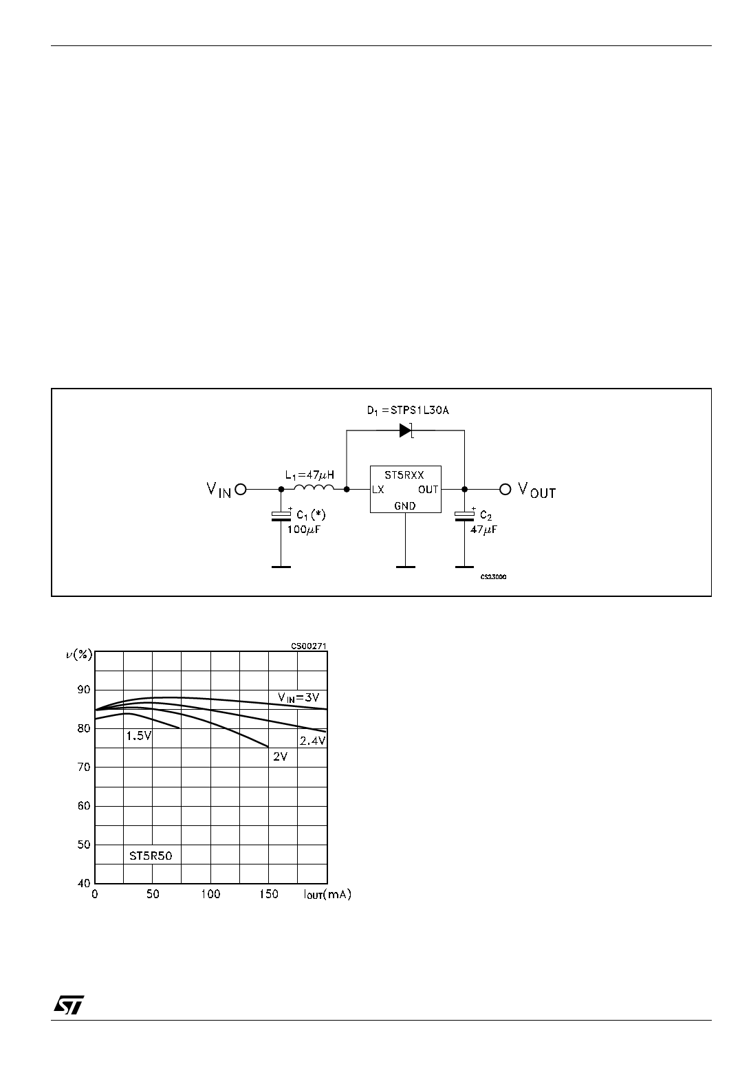
Figure 3: Typical Application Circuit
(*) See application info.
Figure 4: Typical Application Efficiency
3/15
Share Link: 