CS5513-BS(2000) Ver la hoja de datos (PDF) - Cirrus Logic
Número de pieza
componentes Descripción
Lista de partido
CS5513-BS Datasheet PDF : 26 Pages
| |||
CS5510/11/12/13
2. GENERAL DESCRIPTION
The CS5510/11/12/13 are low-cost, easy-to-use,
∆Σ Analog-to-Digital Converters (ADCs) which
use charge balance techniques to achieve 16-bit
(CS5510/11) and 20-bit (CS5512/13) performance.
The ADCs are available in a space efficient 8-pin
SOIC package and are optimized for measuring
signals in weigh scale, process control, and other
industrial applications.
To accommodate these applications, the ADCs in-
clude a fourth order ∆Σ modulator and a digital fil-
ter. When configured with an external master clock
of 32.768 kHz, the filter in the CS5510/12 provides
better than 80 dB of simultaneous 50 and 60 Hz
line rejection, and outputs conversion words at
53.5 Hz. The CS5511/13 include an on-chip oscil-
lator which eliminates the need for an external
clock source.
The CS5510/11/12/13 ADCs are designed to oper-
ate from a single +5 V supply or a variety dual sup-
ply configurations and are optimized to digitize
bipolar signals in industrial applications.
To achieve low cost, the CS5510/11/12/13 family
of converters have no on-chip calibration features.
The CS5510/11/12/13 offer very low offset drift,
low gain drift, and excellent linearity.
2.1 Analog Input
The CS5510/11/12/13 provides a differential input
span of approximately ±(0.80 ± 0.08) times the dif-
ferential voltage reference (VREF - V-). This trans-
lates to typically ±4.0 V fully differential when the
reference voltage between VREF and V- is 5 V,
and typically ±2.0 V fully differential at 2.5 V.
Note:
When a smaller reference voltage is used,
the resulting code widths are smaller. Since
the output codes exhibit more changing
codes for a fixed amount of noise, the
converter appears noisier.
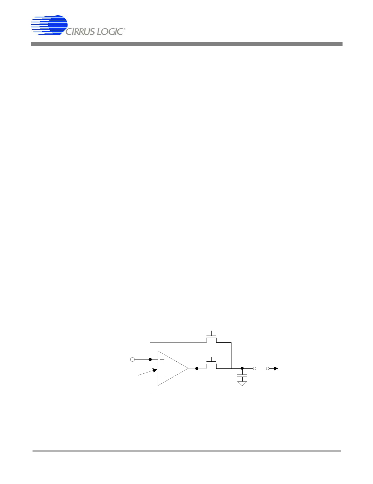
2.1.1 Analog Input Model
Figure 3 illustrates the input model for the AIN
pins. The model includes a coarse/fine charge buff-
er which reduces the dynamic current demands
from the signal source. The buffer is designed to
accommodate rail to rail (common-mode plus sig-
nal) input voltages. Typical CVF (sampling) cur-
rent is about 10 nA. Application Note 30,
“Switched-Capacitor A/D Input Structures”, de-
tails various input architectures.
2.2 Voltage Reference Input
The voltage between the VREF and V- pins of the
converter determines the voltage reference for the
converter. This voltage can be as low as 250 mV, or
AIN
Vo s ≤ 2 5 mV
i n = f Vos C
φ 1 Fine
φ 1 Coarse
C = 12 p F
f = 32.768 kHz
Figure 3. Input models for AIN+ and AIN- pins.
10
DS337F1
Share Link: 