5962R9582401QQC Ver la hoja de datos (PDF) - Intersil
Número de pieza
componentes Descripción
Lista de partido
5962R9582401QQC Datasheet PDF : 16 Pages
| |||
HS-80C85RH
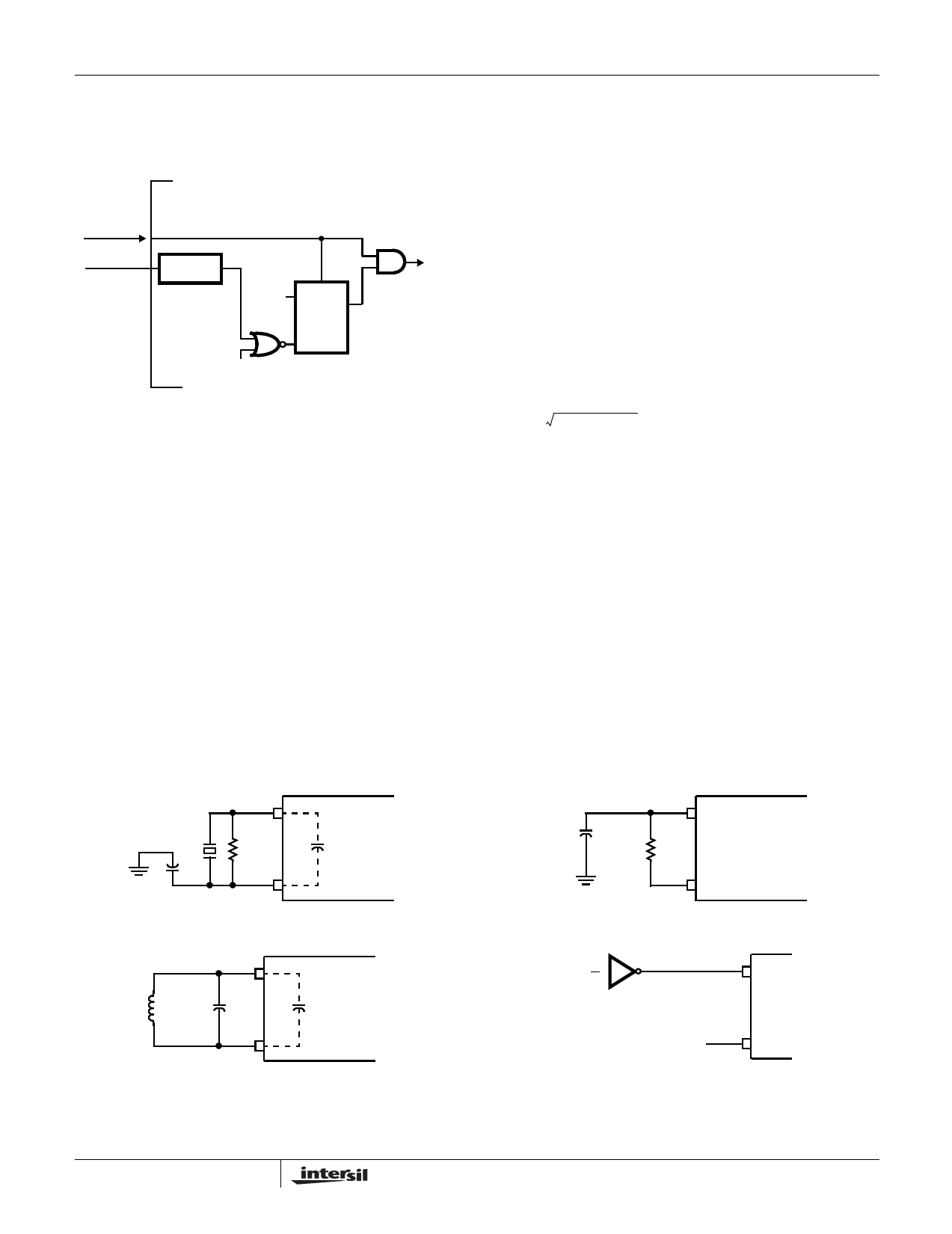
the TRAP interrupt request circuitry within the HS-80C85RH.
Note that the servicing of any interrupt (TRAP, RST 7.5, RST
6.5, RST 5.5, INTR) disables all future interrupts (except
TRAPs) until an EI instruction is executed.
EXTERNAL INSIDE THE
TRAP
80C85RH
INTERRUPT
REQUEST TRAP
RESET IN
SCHMITT RESET
TRIGGER
VDD
D CLK
Q
D
F/F
CLEAR
INTERNAL
TRAP F.F.
TRAP
ACKNOWLEDGE
TRAP
INTERRUPT
REQUEST
FIGURE 8. TRAP AND RESET IN CIRCUIT
The TRAP interrupt is special in that is disables interrupts, but
preserves the previous interrupt enable status. Perform- ing
the first RIM instruction following a TRAP interrupt allows you
to determine whether interrupts were enabled or disabled
prior to the TRAP. All subsequent RIM instructions provide
current interrupt enable status. Performing a RIM instruction
following INTR, or RST 5.5-7.5 will provide current interrupt
enable status, revealing that interrupts are disabled.
The serial I/O system is also controlled by the RIM and SIM
instructions. SID is read by RIM, and SIM sets the SOD data.
Driving the X1 and X2 Inputs
You may drive the clock inputs of the HS-80C85RH with a
crystal, an LC tuned circuit, an RC network, or an external clock
source. The driving frequency may be any value from DC to
4MHz and must be twice the desired internal clock frequency.
The following guidelines should be observed when a crystal
is used to drive the HS-80C85RH clock input:
20pF
X1
1
REXT =
10MΩ
2 X2
80C85RH
CINT =
15pF
1. A 20pF capacitor should be connected from X2 to ground
to assure oscillator start-up at the correct frequency.
2. A 10MΩ resistor is required between X1 and X2 for bias
point stabilization. In addition, the crystal should have the
following characteristics:
1) Parallel resonance at twice the desired internal clock
frequency
2) CL (load capacitance) ≤ 30pF
3) CS (shunt capacitance) ≤ 7pF
4) RS (equivalent shunt resistance) ≤ 75Ω
5) Drive level: 10mW
6) Frequency tolerance: ±0.005% (suggested)
A parallel-resonant LC circuit may be used as the frequency-
determining network for the HS-80C85RH, providing that its
frequency tolerance of approximately ±10% is acceptable.
The components are chosen from the formula:
f = -------------------------1---------------------------
2π L(Cext + Cint)
To minimize variations in frequency, it is recommended that
you choose a value for Cext that is at least twice that of Cint,
or 30pF. The use of an LC circuit is not recommended for
frequencies higher than approximately 4MHz.
An RC circuit may be used as the frequency-determining
network for the HS-80C85RH if maintaining a precise clock
frequency is of no importance. Variations in the on-chip timing
generation can cause a wide variation in frequency when
using the RC mode. Its advantage is its low component cost.
The driving frequency generated by the circuit shown is
approximately 3MHz. It is not recommended that frequencies
greatly higher or lower than this be attempted.
Figure 9 shows the recommended clock driver circuits.
For driving frequencies up to and including 4MHz you may
supply the driving signal to X1 and leave X2 open-circuited
(Figure 9D).
20pF
X1
1
-6K
2 X2
80C85RH
FIGURE 9A. QUARTZ CRYSTAL CLOCK DRIVER
FIGURE 9B. RC CIRCUIT CLOCK DRIVER
LEXT
X1
1
CEXT
2 X2
80C85RH
CINT =
15pF
LOW TIME > 60ns
X1
(NOTE)
X2
NOTE: X2 Left Floating.
FIGURE 9C. LC TUNED CIRCUIT CLOCK DRIVER
FIGURE 9D. 0-4MHz INPUT FREQUENCY EXTERNAL CLOCK
DRIVER CIRCUIT
FIGURE 9. CLOCK DRIVER CIRCUITS
11
Share Link: 