74LV251 Ver la hoja de datos (PDF) - Philips Electronics
Número de pieza
componentes Descripción
Lista de partido
74LV251 Datasheet PDF : 12 Pages
| |||
Philips Semiconductors
8-input multiplexer (3-State)
Product specification
74LV251
AC WAVEFORMS
VM = 1.5 V at VCC ≥ 2.7 V
VM = 0.5 V × VCC at VCC < 2.7 V
VOL and VOH are the typical output voltage drop that occur with the
output load.
VX = VOL + 0.3 V at VCC ≥ 2.7 V
VX = VOL + 0.1 × VCC at VCC < 2.7 V
VY = VOH – 0.3 V at VCC ≥ 2.7V
VY = VOH – 0.1 × VCC at VCC < 2.7 V
V CC
In , Sn INPUT
GND
V OH
tPHL
Y OUTPUT
VM
VM
tPLH
V OL
SV00633
Figure 1. Multiplexer input (In) and select input (Sn) to
output (Y) propagation delays.
V CC
In, Sn INPUT
GND
tPHL
V OH
Y OUTPUT
VM
VM
tPLH
V OL
SV00634
Figure 2. Multiplexer input (In) and the select input (Sn) to
output (Y) propagation delays.
VCC
OE INPUT
VM
GND
VCC
OUTPUT
LOW-to-OFF
OFF-to-LOW
VOL
tPLZ
VX
tPHZ
tPZL
VM
tPZH
VOH
OUTPUT
HIGH-to-OFF
OFF-to-HIGH
GND
outputs
enabled
VY
outputs
disabled
VM
outputs
enabled
SV00635
Figure 3. 3-State enable and disable times
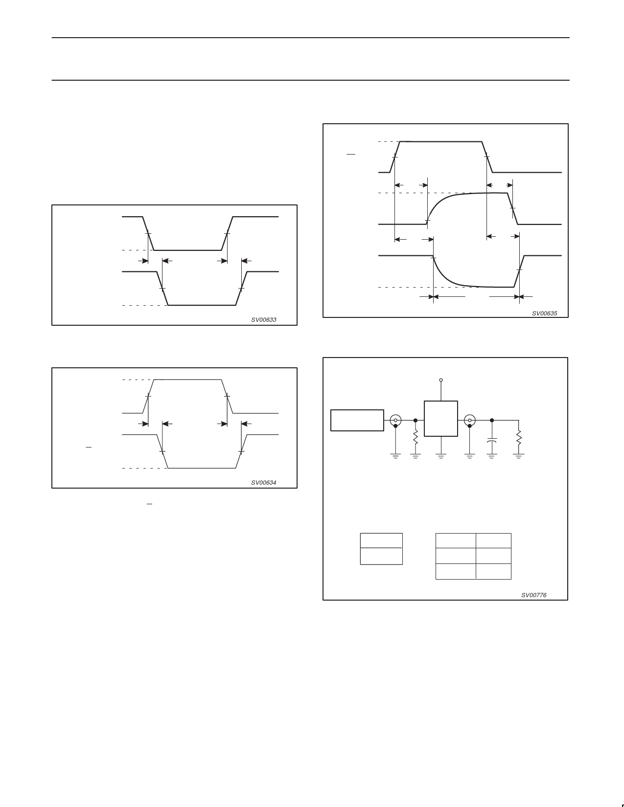
TEST CIRCUIT
VCC
PULSE
GENERATOR
VI
RT
D.U.T.
VO
50pF
CL
RL= 1KΩ
Test Circuit for switching times
DEFINITIONS
RT = Termination resistance should be equal to ZOUT of pulse generators.
RL = Load resistor
CL = Load capacitance includes jig and probe capacitance
TEST
tPLH/tPHL
VCC
< 2.7V
2.7–3.6V
VI
VCC
2.7V
SV00776
Figure 4. Load circuitry for switching times.
1998 May 20
7
Share Link: 