A43L2632V-6 Ver la hoja de datos (PDF) - AMIC Technology
Número de pieza
componentes Descripción
Lista de partido
A43L2632V-6 Datasheet PDF : 43 Pages
| |||
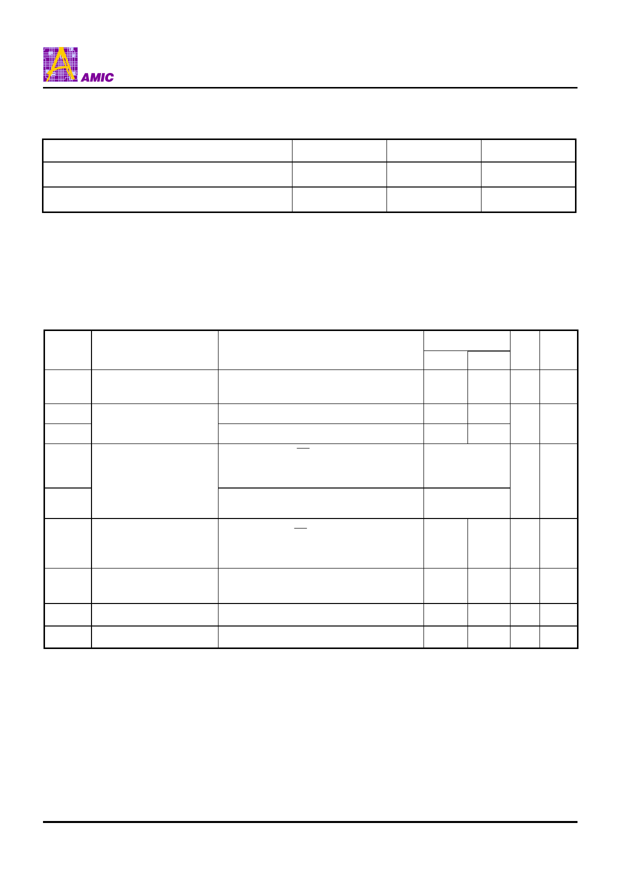
Decoupling Capacitance Guide Line
Recommended decoupling capacitance added to power line at board.
Parameter
Symbol
Decoupling Capacitance between VDD and VSS
CDC1
Decoupling Capacitance between VDDQ and VSSQ
CDC2
Note: 1. VDD and VDDQ pins are separated each other.
All VDD pins are connected in chip. All VDDQ pins are connected in chip.
2. VSS and VSSQ pins are separated each other
All VSS pins are connected in chip. All VSSQ pins are connected in chip.
Value
0.1 + 0.01
0.1 + 0.01
A43L2632
Unit
µF
µF
DC Electrical Characteristics
(Recommended operating condition unless otherwise noted, TA = 0 to 70°C or TA = -40ºC to +85ºC )
Symbol
Parameter
Test Conditions
Icc1
Icc2 P
Icc2 PS
Operating Current
(One Bank Active)
Burst Length = 1
tRC ≥ tRC(min), tCC ≥ tCC(min), IOL = 0mA
Precharge Standby Current CKE ≤ VIL(max), tCC = 15ns
in power-down mode
CKL ≤ VIL(max), tCC = ∞
Speed
-6
-7
85
80
45
40
3
3
ICC2N
ICC2NS
ICC3N
ICC4
Precharge Standby Current
in non power-down mode
CKE ≥ VIH(min), CS ≥ VIH(min), tCC = 15ns
Input signals are changed one time during
30ns
CKE ≥ VIH(min), CLK ≤ VIL(max), tCC = ∞
Input signals are stable.
Active Standby current in
non power-down mode
(One Bank Active)
CKE ≥ VIH(min), CS ≥ VIH(min), tCC = 15ns
Input signals are changed one time during
30ns
Operating Current
(Burst Mode)
IOL = 0mA, Page Burst
All bank Activated, tCCD = tCCD (min)
8
1
65
60
200
170
ICC5
ICC6
Refresh Current
Self Refresh Current
tRC ≥ tRC (min)
CKE = 0.2V
180
170
3
3
Note: 1. Measured with outputs open. Addresses are changed only one time during tCC(min).
2. Refresh period is 64ms. Addresses are changed only one time during tCC(min).
Unit Notes
mA
1
mA
mA
mA
mA
1
mA
2
mA
PRELIMINARY (January, 2005, Version 0.0)
6
AMIC Technology, Corp.
Share Link: 