A49LF040TL-33F Ver la hoja de datos (PDF) - AMIC Technology
Número de pieza
componentes Descripción
Lista de partido
A49LF040TL-33F Datasheet PDF : 31 Pages
| |||
A49LF040
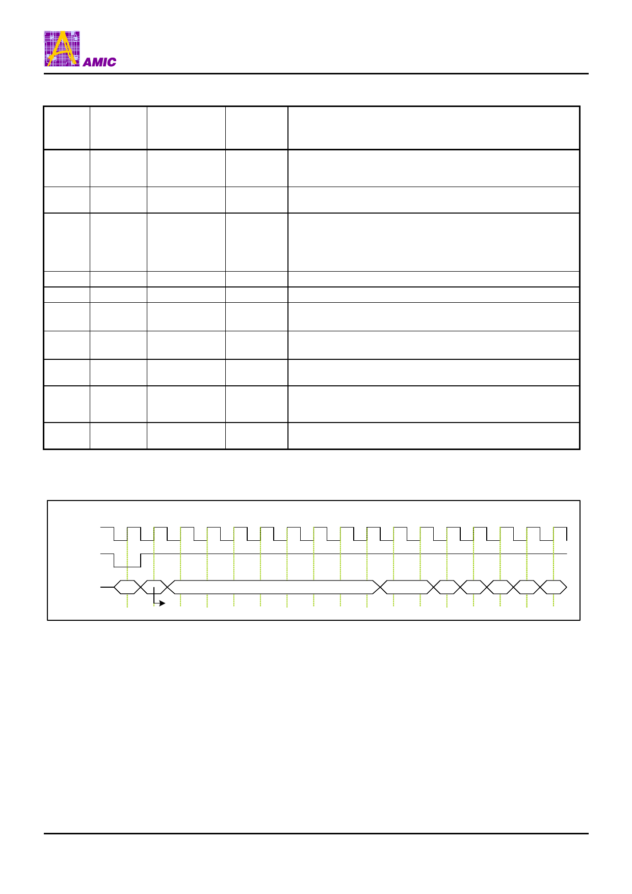
Table 3: LPC Write Cycle
Clock
Cycle
Field
Name
Field Contents LAD[3:0]
LAD[3:0]1
Direction
Comments
1
START
2
CYCTYPE
+ DIR
0000
010X
3-10 ADDRESS
YYYY
11
DATA
12
DATA
13
TAR0
ZZZZ
ZZZZ
1111
14
TAR1
1111(float)
15
SYNC
0000
16
TAR0
1111
17
TAR1
1111(float)
IN
IN
IN
IN
IN
IN
then Float
Float
then OUT
OUT
OUT
then Float
Float
then IN
LFRAME# must be active (low) for the part to respond. Only the last
start field (before LFRAME# transitioning high) should be
recognized.
Indicates the type of cycle. Bits 3:2 must be “01b” for memory cycle.
Bit 1 indicates the type of transfer “1” for Write. Bit 0 is reserved.
Address Phase for Memory Cycle. LPC protocol supports a 32-bit
address phase. YYYY is one nibble of the entire address.
Addresses are transferred most-significant nibble first. See Table 4
for address bits definition and Table 5 for valid memory address
range.
This field is the least-significant nibble of the data byte.
This field is the most-significant nibble of the data byte.
In this clock cycle, the host has driven the bus to all ‘1’s and then
floats the bus. This is the first part of the bus “turnaround cycle.”
The A49LF040 takes control of the bus during this cycle.
The A49LF040 outputs the values 0000, indicating that it has
received data or a flash command.
In this clock cycle, the A49LF040 has driven the bus to all ‘1’s and
then floats the bus. This is the first part of the bus “turnaround
cycle.”
Host resumes control of the bus during this cycle.
1. Field contents are valid on the rising edge of the present clock cycle.
LPC Write Waveforms
LCLK
1
2
3
4
5
6
7
8
9
10 11 12 13 14 15 16 17
LFRAME#
LAD[3:0]
START
CYCTYPE
+ DIR
ADDRESS
DATA
TAR0 TAR1 SYNC TAR0 TAR1
PRELIMINARY (August, 2004, Version 0.1)
7
AMIC Technology, Corp.
Share Link: 