A49LF040ATL-33 Ver la hoja de datos (PDF) - AMIC Technology
Número de pieza
componentes Descripción
Lista de partido
A49LF040ATL-33 Datasheet PDF : 32 Pages
| |||
A49LF040A
ADDRESS/ADDRESS MULTIPLEXED (A/A MUX)
MODE
Device Operation
Commands are used to initiate the memory operation
functions of the device. The data portion of the software
command sequence is latched on the rising edge of WE .
During the software command sequence the row address is
latched on the falling edge of R/C and the column address is
latched on the rising edge of R/C . Refer to Table 10 and
Table 11 for operation modes and the command sequence.
Read
The Read operation of the A49LF040A device is controlled
by OE . OE is the output control and is used to gate data
from the output pins. Refer to the Read cycle timing diagram,
Figure 10 for further details.
Reset
A VIL on RST pin initiates a device reset.
Byte-Program Operation
The A49LF040A device is programmed on a byte-by-byte
basis. Before programming, one must ensure that the block,
in which the byte which is being programmed exists, is fully
erased. The Byte-Program operation is initiated by executing
a four-byte command load sequence for Software Data
Protection with address and data in the last byte sequence.
During the Byte-Program operation, the row address (A10-A0)
is latched on the falling edge of R/C and the column Address
(A18-A11) is latched on the rising edge of R/C . The data bus
is latched in the rising edge of WE . See Figure 11 for
Program operation timing diagram, Figure 14 for timing
waveforms, and Figure 19 for its flowchart. During the
Program operation, the only valid reads are Data Polling and
Toggle Bit. During the internal Program operation, the host is
free to perform additional tasks. Any commands written
during the internal Program operation will be ignored.
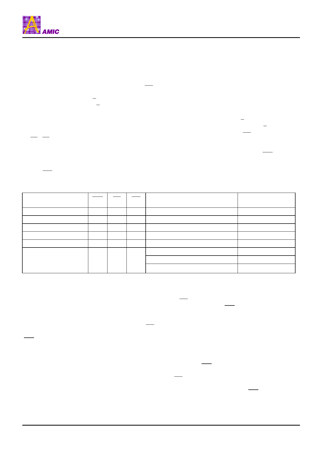
Table 10: A/A Mux Mode Operation Selection
Mode
RST OE WE
Read
Write
Standby
Output Disable
Reset
VIH
VIL
VIH
VIH
VIH
VIL
VIH
VIH
VIH
VIH
VIH
X
VIL
X
X
Product Identification
VIH
VIL
VIH
Address
AIN
AIN
X
X
X
A18 – A2 = X, A1 = VIL, A0 = VIL
A18 – A2 = X, A1 = VIL, A0 = VIH
A18 – A2 = X, A1 = VIH, A0 = VIH
I/O
DOUT
DIN
High Z
High Z
High Z
Manufacturer ID
Device ID
Continuation ID
Block-Erase Operation
The Block-Erase Operation allows the system to erase the
device in 64 KByte uniform block size for the A49LF040A.
The Block-Erase operation is initiated by executing a six-byte
command load sequence for Software Data Protection with
Block-Erase command (30H or 50H) and block address. The
internal Block-Erase operation begins after the sixth WE
pulse. The End-of-Erase can be determined using either
Data Polling or Toggle Bit methods. See Figure 15 for timing
waveforms. Any commands written during the Block- Erase
operation will be ignored.
Chip-Erase
The A49LF040A device provides a Chip-Erase operation
only in A/A Mux mode, which allows the user to erase the
entire memory array to the ‘1’s state. This is useful when the
entire device must be quickly erased. The Chip-Erase
operation is initiated by executing a six-byte Software Data
Protection command sequence with Chip-Erase command
(10H) with address 5555H in the last byte sequence. The
internal Erase operation begins with the rising edge of the
sixth WE . During the internal Erase operation, the only
valid read is Toggle Bit or Data Polling. See Table 11 for the
command sequence, Figure 16 for timing diagram, and
Figure 21 for the flowchart. Any commands written during the
Chip-Erase operation will be ignored.
Write Operation Status Detection
The A49LF040A device provides two software means to
detect the completion of a Write cycle, in order to optimize
the system Write cycle time. The software detection includes
two status bits: Data Polling (I/O7) and Toggle Bit (I/O6). The
End-of-Write detection mode is enabled after the rising edge
of WE which initiates the internal Write operation. The
actual completion of the nonvolatile write is asynchronous
with the system; therefore, either a Data Polling or Toggle
Bit read may be simultaneous with the completion of the
Write cycle.
PRELIMINARY (March, 2006, Version 0.1)
12
AMIC Technology, Corp.
Share Link: 