AD2S105AP Ver la hoja de datos (PDF) - Analog Devices
Número de pieza
componentes Descripción
Lista de partido
AD2S105AP Datasheet PDF : 12 Pages
| |||
AD2S105
TIMING DIAGRAMS
Busy Output
The BUSY output will go HI at the negative edge of the
STROBE input. This is used to synchronize digital input data
and load the digital angular rotation information into the device
counter. The BUSY output will remain HI for 2 µs, and go LO
until the next strobe negative edge occurs.
Strobe Input
The width of the positive STROBE pulse should be at least
100 ns, in order to successfully start the conversion. The maxi-
mum frequency of STROBE input is 366 kHz, i.e., there should
be at least 2.73 µs from the negative edge of one STROBE pulse
to the next rising edge. This is illustrated by the following tim-
ing diagram and table.
STROBE
BUSY
t1
t2
tr
t4
tf
t3
Figure 7. AD2S105 Timing Diagram
Note: Digital data should be stable 25 ns before and after posi-
tive strobe edge.
Table II. AD2S105 Timing Table
Parameter Min Typ Max Condition
t1
100 ns
STROBE Pulse Width
t2
30 ns
STROBE ↓ to BUSY ↑
t3
1.7 µs
2.5 µs BUSY Pulse Width
t4
100 ns
BUSY ↓ to STROBE ↑
tr
20 ns
BUSY Pulse Rise Time
with No Load
150 ns
BUSY Pulse Rise Time
with 68 pF Load
tf
10 ns
BUSY Pulse Fall Time
with No Load
120 ns
BUSY Pulse Fall Time
with 68 pF Load
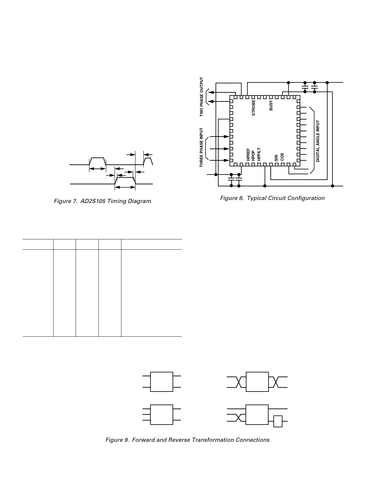
TYPICAL CIRCUIT CONFIGURATION
Figure 8 shows a typical circuit configuration for the AD2S105
in a three phase, nominal level input mode (MODE2).
100nF
10µF
+5V
PH/OP1
1
41
MSB
38
AGND
PH/IP4
12
PH/IP3
AD2S105
TOP VIEW
34
PH/IP2
16
PH/IP1
23
30
27
–5V
100nF
10µF
LSB
GND
Figure 8. Typical Circuit Configuration
APPLICATIONS
Transformation Configuration
The AD2S105 can perform both forward and reverse transfor-
mations. The section “Theory of Operation” explains how the
chip operates with the core operator e+j, which performs a for-
ward transformation. The reverse transformation, e–j, is per-
formed by providing a negative angle φ. Figure 9 shows two
different phase input/output connections for AD2S105 reverse
transformation operation.
2 PHASE – 2 PHASE
FORWARD
TRANSFORMATION
AD2S105
Cosθ
Sinθ
e+jφ
Cos(θ + φ)
Sin(θ + φ)
REVERSE
TRANSFORMATION
AD2S105
Cosθ
Sinθ
e–jφ
Cos(θ – φ)
Sin(θ – φ)
3 PHASE – 2 PHASE
Cosθ
Cos(θ + 120°)
Cos(θ + 240°)
e+jφ
Cos(θ + φ)
Sin(θ + φ)
Cosθ
Cos(θ + 120°)
Cos(θ + 240°)
e–jφ
Cos(θ – φ)
Sin(θ – φ)
–1
Figure 9. Forward and Reverse Transformation Connections
–8–
REV. 0
Share Link: 