EVAL-ADF4193EB1(RevB) Ver la hoja de datos (PDF) - Analog Devices
Número de pieza
componentes Descripción
Lista de partido
EVAL-ADF4193EB1 Datasheet PDF : 28 Pages
| |||
ADF4193
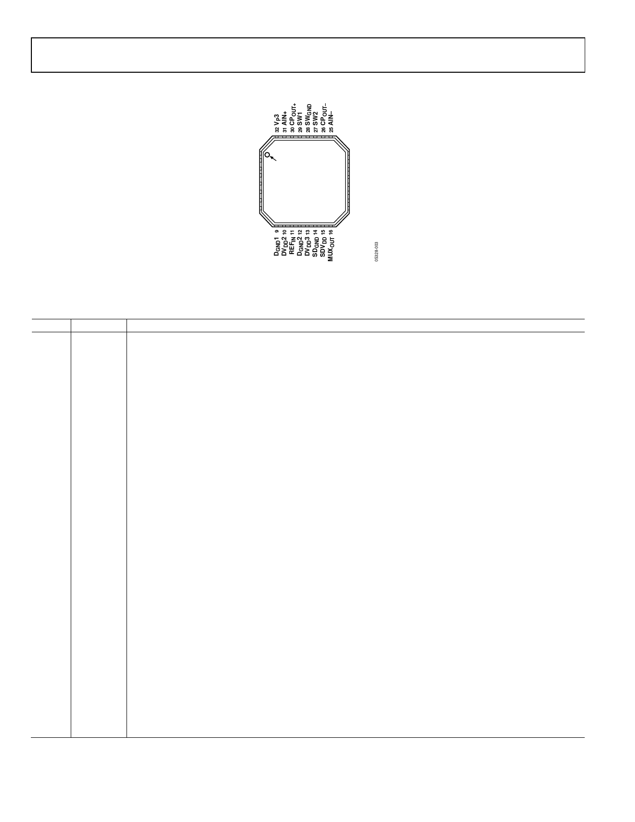
PIN CONFIGURATION AND FUNCTION DESCRIPTIONS
CMR 1
AOUT 2
SW3 3
AGND1 4
RFIN– 5
RFIN+ 6
AVDD1 7
DVDD1 8
PIN 1
INDICATOR
ADF4193
TOP VIEW
24 VP2
23 RSET
22 AGND2
21 DGND3
20 VP1
19 LE
18 DATA
17 CLK
Figure 3. Pin Configuration
Table 4. Pin Function Descriptions
Pin No. Mnemonic Description
1
CMR
Common-Mode Reference Voltage for the Differential Amplifier’s Output Voltage Swing. Internally biased to
three-fifths of VP3. Requires a 0.1 μF capacitor to ground.
2
AOUT
Differential Amplifier Output to Tune the External VCO.
3
SW3
Fast-Lock Switch 3. Closed while SW3 timeout counter is active.
4
AGND1
Analog Ground. This is the ground return pin for the differential amplifier and the RF section.
5
RFIN−
Complementary Input to the RF Prescaler. This point must be decoupled to the ground plane with a small bypass
capacitor, typically 100 pF.
6
RFIN+
Input to the RF Prescaler. This small signal input is ac-coupled to the external VCO.
7
AVDD1
Power Supply Pin for the RF Section. Nominally 3 V. A 100 pF decoupling capacitor to the ground plane should be
placed as close as possible to this pin.
8
DVDD1
Power Supply Pin for the N Divider. Should be the same voltage as AVDD1. A 0.1 μF decoupling capacitor to ground
should be placed as close as possible to this pin.
9
DGND1
Ground Return Pin for DVDD1.
10
DVDD2
Power Supply Pin for the REFIN Buffer and R Divider. Nominally 3 V. A 0.1 μF decoupling capacitor to ground
should be placed as close as possible to this pin.
11
REFIN
Reference Input. This is a CMOS input with a nominal threshold of VDD/2 and a dc equivalent input resistance of
100 kΩ (see Figure 15). This input can be driven from a TTL or CMOS crystal oscillator or it can be ac-coupled.
12
DGND2
Ground Return Pin for DVDD2 and DVDD3.
13
DVDD3
Power Supply Pin for the Serial Interface Logic. Nominally 3 V.
14
SDGND
Ground Return Pin for the Σ-Δ Modulator.
15
SDVDD
Power Supply Pin for the Digital Σ-Δ Modulator. Nominally 3 V. A 0.1 μF decoupling capacitor to the ground plane
should be placed as close as possible to this pin.
16
MUXOUT
Multiplexer Output. This multiplexer output allows either the lock detect, the scaled RF, or the scaled reference
frequency to be accessed externally (see Figure 35).
17
CLK
Serial Clock Input. Data is clocked into the 24-bit shift register on the CLK rising edge. This input is a high
impedance CMOS input.
18
DATA
Serial Data Input. The serial data is loaded MSB first with the three LSBs as the control bits. This input is a high
impedance CMOS input.
19
LE
Load Enable, CMOS Input. When LE goes high, the data stored in the shift register is loaded into the register that is
selected by the three LSBs.
20
VP1
Power Supply Pin for the Phase Frequency Detector (PFD). Nominally 5 V, should be at the same voltage at VP2.
A 0.1 μF decoupling capacitor to ground should be placed as close as possible to this pin.
21
DGND3
Ground Return Pin for VP1.
22
AGND2
Ground Return Pin for VP2.
Rev. B | Page 6 of 28
Share Link: 