ADL5562 Ver la hoja de datos (PDF) - Analog Devices
Número de pieza
componentes Descripción
Lista de partido
ADL5562 Datasheet PDF : 21 Pages
| |||
Data Sheet
FEATURES
−3 dB bandwidth of 3.3 GHz (AV = 6 dB)
Pin-strappable gain adjust: 6 dB, 12 dB, 15.5 dB
Differential or single-ended input to differential output
Low noise input stage: 2.1 nV/√Hz RTI at AV = 12 dB
Low broadband distortion (AV = 6 dB)
10 MHz: −91 dBc HD2, −98 dBc HD3
70 MHz: −102 dBc HD2, −90 dBc HD3
140 MHz: −104 dBc HD2, −87 dBc HD3
250 MHz: −80 dBc HD2, −94 dBc HD3
IMD3s of −94 dBc at 250 MHz center
Slew rate: 9.8 V/ns
Fast settling of 2 ns and overdrive recovery of 3 ns
Single-supply operation: 3 V to 3.6 V
Power-down control
Fabricated using the high speed XFCB3 SiGe process
APPLICATIONS
Differential ADC drivers
Single-ended to differential conversion
RF/IF gain blocks
SAW filter interfacing
GENERAL DESCRIPTION
The ADL5562 is a high performance differential amplifier
optimized for RF and IF applications. The amplifier offers low
noise of 2.1 nV/√Hz and excellent distortion performance over
a wide frequency range, making it an ideal driver for high speed
8-bit to 16-bit ADCs.
The ADL5562 provides three gain levels of 6 dB, 12 dB, and
15.5 dB through a pin-strappable configuration. For the single-
ended input configuration, the gains are reduced to 5.6 dB,
11.1 dB, and 14.1 dB. Using an external series input resistor
expands the amplifier gain flexibility and allows for any gain
selection from 0 dB to 15.5 dB.
The quiescent current of the ADL5562 is typically 80 mA and,
when disabled, consumes less than 3 mA, offering excellent
input-to-output isolation.
3.3 GHz Ultralow Distortion
RF/IF Differential Amplifier
ADL5562
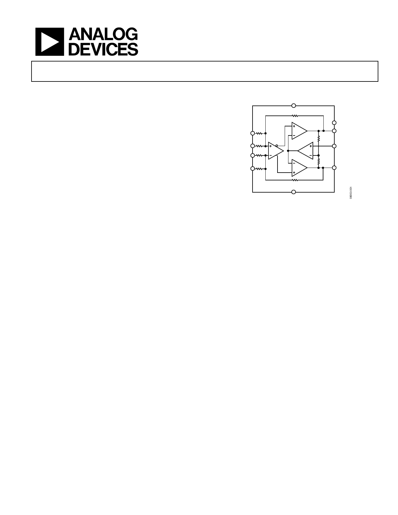
FUNCTIONAL BLOCK DIAGRAM
VCC
RF
RG2
VIP2
RG1
VIP1
RG1
VIN1
RG2
VIN2
ENBL
VON
VCOM
VOP
RF ADL5562
GND
Figure 1.
The device is optimized for wideband, low distortion
performance. These attributes, together with its adjustable gain
capability, make this device the amplifier of choice for general-
purpose IF and broadband applications where low distortion,
noise, and power are critical. This device is optimized for the
best combination of slew speed, bandwidth, and broadband
distortion. These attributes allow it to drive a wide variety of
analog-to-digital converters (ADCs) and make it ideally suited
for driving mixers, pin diode attenuators, SAW filters, and
multi-element discrete devices.
Fabricated on an Analog Devices, Inc., high speed SiGe process,
the ADL5562 is supplied in a compact 3 mm × 3 mm, 16-lead
LFCSP package and operates over the temperature range of
−40°C to + 85°C.
Rev. F
Document Feedback
Information furnished by Analog Devices is believed to be accurate and reliable. However, no
responsibility is assumed by Analog Devices for its use, nor for any infringements of patents or other
rights of third parties that may result from its use. Specifications subject to change without notice. No
license is granted by implication or otherwise under any patent or patent rights of Analog Devices.
Trademarks and registered trademarks are the property of their respective owners.
One Technology Way, P.O. Box 9106, Norwood, MA 02062-9106, U.S.A.
Tel: 781.329.4700 ©2009–2017 Analog Devices, Inc. All rights reserved.
Technical Support
www.analog.com
Share Link: 