ADP1173 Ver la hoja de datos (PDF) - Analog Devices
Número de pieza
componentes Descripción
Lista de partido
ADP1173 Datasheet PDF : 16 Pages
| |||
ADP1173
ABSOLUTE MAXIMUM RATINGS*
Supply Voltage (VIN) . . . . . . . . . . . . . . . . . . . . . . . . . . . . 36 V
SW1 Pin Voltage (VSW1) . . . . . . . . . . . . . . . . . . . . . . . . . 50 V
SW2 Pin Voltage (VSW2) . . . . . . . . . . . . . . . . . . –0.5 V to VIN
Feedback Pin Voltage (ADP1173) . . . . . . . . . . . . . . . . . . . 5 V
Sense Pin Voltage (ADP1173, –3.3, –5, –12) . . . . . . . . . 36 V
Maximum Power Dissipation . . . . . . . . . . . . . . . . . . 500 mW
Maximum Switch Current . . . . . . . . . . . . . . . . . . . . . . . .1.5 A
Operating Temperature Range . . . . . . . . . . . . . 0°C to +70°C
Storage Temperature Range . . . . . . . . . . . . . –65°C to 150°C
Lead Temperature, (Soldering, 10 sec) . . . . . . . . . . . . +300°C
*Stresses above those listed under Absolute Maximum Ratings may cause perma-
nent damage to the device. This is a stress rating only; functional operation of the
device at these or any other conditions above those listed in the operational
sections of this specification is not implied. Exposure to absolute maximum
ratings for extended periods of time may affect device reliability.
ORDERING GUIDE
Model
ADP1173AN
ADP1173AR
ADP1173AN-3.3
ADP1173AR-3.3
ADP1173AN-5
ADP1173AR-5
ADP1173AN-12
ADP1173AR-12
Output
Voltage
ADJ
ADJ
3.3 V
3.3 V
5V
5V
12 V
12 V
*N = Plastic DIP, SO = Small Outline Package.
Package
Options*
N-8
SO-8
N-8
SO-8
N-8
SO-8
N-8
SO-8
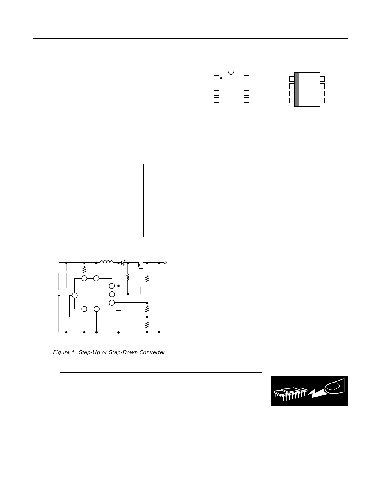
4X NICAD
OR
ALKALINE
CELLS
L1*
100µH
+
470µF
56Ω
1
2
ILIM VIN SW1 3
ADP1173
7 SET
AO 6
IRF7203
470kΩ
75kΩ
+5V
OUTPUT
AT 100mA
+
470µF
GND
5
SW2 FB 8
4
+
240Ω
470µF
24kΩ
*L1 = COILTRONICS CTX100-4
Figure 1. Step-Up or Step-Down Converter
PIN CONFIGURATIONS
N-8
8-Lead Plastic DIP
SO-8
8-Lead Plastic SO
ILIM 1
8 FB (SENSE)*
VIN 2 ADP1173 7 SET
SW1
3
TOP VIEW
(Not to Scale)
6
AO
SW2 4
5 GND
*FIXED VERSIONS
ILIM 1
VIN 2
SW1 3
SW2 4
8 FB (SENSE)*
ADP1173 7 SET
TOP VIEW
(Not to Scale) 6 AO
5 GND
*FIXED VERSIONS
PIN FUNCTION DESCRIPTIONS
Mnemonic Function
ILIM
VIN
SW1
SW2
GND
AO
SET
FB/SENSE
For normal conditions this pin is connected to
VIN. When lower current is required, a resistor
should be connected between ILIM and VIN.
Limiting the switch current to 400 mA is
achieved by connecting a 220 Ω resistor.
Input Voltage.
Collector Node of Power Transistor.
For step-down configuration, connect to VIN;
for step-up configuration, connect to an
inductor/diode.
Emitter Node of Power Transistor. For step-
down configuration, connect to inductor/
diode; for step-up configuration, connect to
ground. Do not allow this pin to drop more
than a diode drop below ground.
Ground.
Auxiliary Gain (GB) Output. The open
collector can sink 100 µA.
Gain Amplifier Input. The amplifier has
positive input connected to the SET pin and
negative input is connected to 1.245 V
reference.
On the ADP1173 (adjustable) version this pin
is connected to the comparator input. On the
ADP1173-3.3, ADP1173-5 and ADP1173-12,
the pin goes directly to the internal application
resistor that sets the output voltage.
CAUTION
ESD (electrostatic discharge) sensitive device. Electrostatic charges as high as 4000 V readily
accumulate on the human body and test equipment and can discharge without detection.
Although the ADP1173 features proprietary ESD protection circuitry, permanent damage may
occur on devices subjected to high energy electrostatic discharges. Therefore, proper ESD
precautions are recommended to avoid performance degradation or loss of functionality.
WARNING!
ESD SENSITIVE DEVICE
REV. 0
–3–
Share Link: 