AOZ1014 Ver la hoja de datos (PDF) - Alpha and Omega Semiconductor
Número de pieza
componentes Descripción
Lista de partido
AOZ1014 Datasheet PDF : 21 Pages
| |||
^lwNMNQ
Ordering Information
Part Number
AOZ1014AI
AOZ1014DI
Ambient Temperature Range
-40°C to +85°C
-40°C to +85°C
Package
SO-8
DFN-8
Environmental
RoHS
RoHS
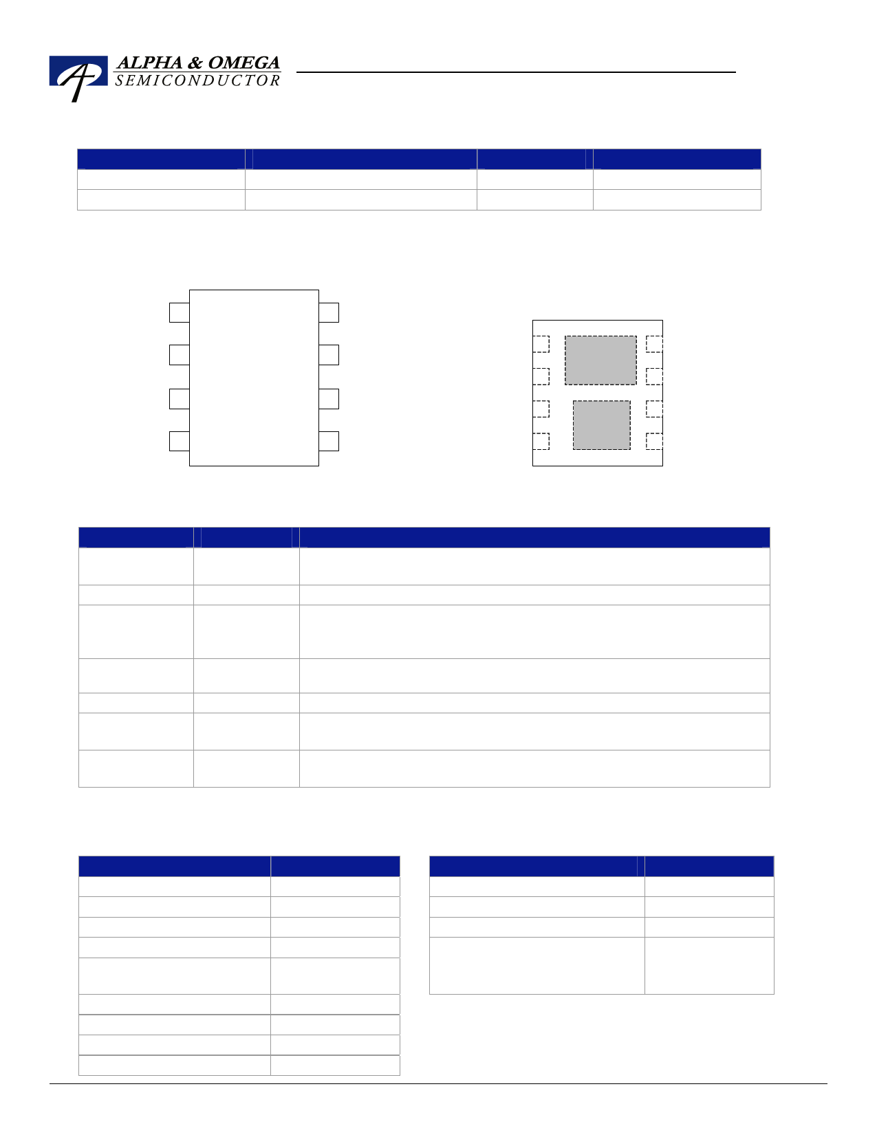
Pin Configuration
VIN 1
PGND 2
SO-8
8
7
AGND 3
6
FB 4
5
LX
LX
EN
COMP
VIN 1
PGND 2
AGND 3
FB 4
DFN-8
LX
AGND
8 LX
7 LX
6 EN
5 COMP
Pin Description
Pin Number
1
Pin Name
VIN
2
PGND
3
AGND
4
FB
5
COMP
6
EN
7,8
LX
Pin Function
Supply voltage input. When VIN rises above the UVLO threshold the
device starts up.
Power ground. Electrically needs to be connected to AGND.
Reference connection for controller section. Also used as thermal
connection for controller section. Electrically needs to be connected
to PGND.
The FB pin is used to determine the output voltage via a resistor
divider between the output and GND.
External loop compensation pin.
The enable pin is active high. Connect EN pin to VIN if not used. Do
not leave the EN pin floating.
PWM output connection to inductor. Thermal connection for output
stage.
Absolute Maximum Ratings(1)
Recommend Operating Ratings(2)
Parameter
Supply Voltage (VIN)
LX to AGND
EN to AGND
FB to AGND
COMP to AGND
PGND to AGND
Junction Temperature (TJ)
Storage Temperature (TS)
ESD Rating(3)
Units
18V
-0.7V to VIN+0.3V
-0.3V to VIN+0.3V
-0.3V to 6V
-0.3V to 6V
-0.3V to +0.3V
+150°C
-65°C to +150°C
2kV
Parameter
Supply Voltage (VIN)
Output Voltage Range
Ambient Temperature (TA)
Package Thermal Resistance
SO-8 (ΘJA)
DFN-8 (ΘJA)
Units
4.5V to 16V
0.8V to VIN
-40°C to +85°C
82° C/W
50° C/W
February 2006
www.aosmd.com
Page 2 of 21
Share Link: 