AOZ1014 Ver la hoja de datos (PDF) - Alpha and Omega Semiconductor
Número de pieza
componentes Descripción
Lista de partido
AOZ1014 Datasheet PDF : 21 Pages
| |||
Detailed Description
The AOZ1014 is a current-mode step down regulator
with integrated high side PMOS switch and a low side
freewheeling Schottky diode. It operates from a 4.5V to
16V input voltage range and supplies up to 5A of load
current. The duty cycle can be adjusted from 6% to
100% allowing a wide range of output voltage. Features
include enable control, Power-On Reset, input under
voltage lockout, fixed internal soft-start and thermal
shut down.
The AOZ1014 is available in SO-8 and thermally
enhanced DFN-8 package.
Enable and Soft Start
The AOZ1014 has internal soft start feature to limit in-
rush current and ensure the output voltage ramps up
smoothly to regulation voltage. A soft start process
begins when the input voltage rises to 4.0V and voltage
on EN pin is HIGH. In soft start process, the output
voltage is ramped to regulation voltage in typically 4ms.
The 4ms soft start time is set internally.
The EN pin of the AOZ1014 is active high. Connect the
EN pin to VIN if enable function is not used. Pull it to
ground will disable the AOZ1014. Do not leave it open.
The voltage on EN pin must be above 2.0 V to enable
the AOZ1014. When voltage on EN pin falls below 0.6 V,
the AOZ1014 is disabled. If an application circuit
requires the AOZ1014 to be disabled, an open drain or
open collector circuit should be used to interface to EN
pin.
Steady-State Operation
Under steady-state conditions, the converter operates
in fixed frequency and Continuous-Conduction Mode
(CCM).
The AOZ1014 integrates an internal P-MOSFET as the
high-side switch. Inductor current is sensed by
amplifying the voltage drop across the drain to source
of the high side power MOSFET. Output voltage is
divided down by the external voltage divider at the FB
pin. The difference of the FB pin voltage and reference
is amplified by the internal transconductance error
amplifier. The error voltage, which shows on the COMP
pin, is compared against the current signal, which is
sum of inductor current signal and ramp compensation
signal, at PWM comparator input. If the current signal is
less than the error voltage, the internal high-side switch
is on. The inductor current flows from the input through
the inductor to the output. When the current signal
exceeds the error voltage, the high-side switch is off.
The inductor current is freewheeling through the
external Schottky diode to output.
^lwNMNQ
The AOZ1014 uses a P-Channel MOSFET as the high
side switch. It saves the bootstrap capacitor normally
seen in a circuit which is using an NMOS switch. It
allows 100% turn-on of the upper switch to achieve
linear regulation mode of operation. The minimum
voltage drop from VIN to VO is the load current times DC
resistance of MOSFET plus DC resistance of buck
inductor. It can be calculated by equation below:
VO _ MAX = VIN − IO × (RDS (ON ) + Rinductor )
Where VO_MAX is the maximum output voltage;
VIN is the input voltage from 4.5V to 16V;
IO is the output current from 0A to 5A;
RDS(ON) is the on resistance of internal
MOSFET, the value is between 25mΩ and
55mΩ depending on input voltage and junction
temperature;
Rinductor is the inductor DC resistance;
Switching Frequency
The AOZ1014 switching frequency is fixed and set by
an internal oscillator. The practical switching frequency
could range from 350kHz to 600kHz due to device
variation.
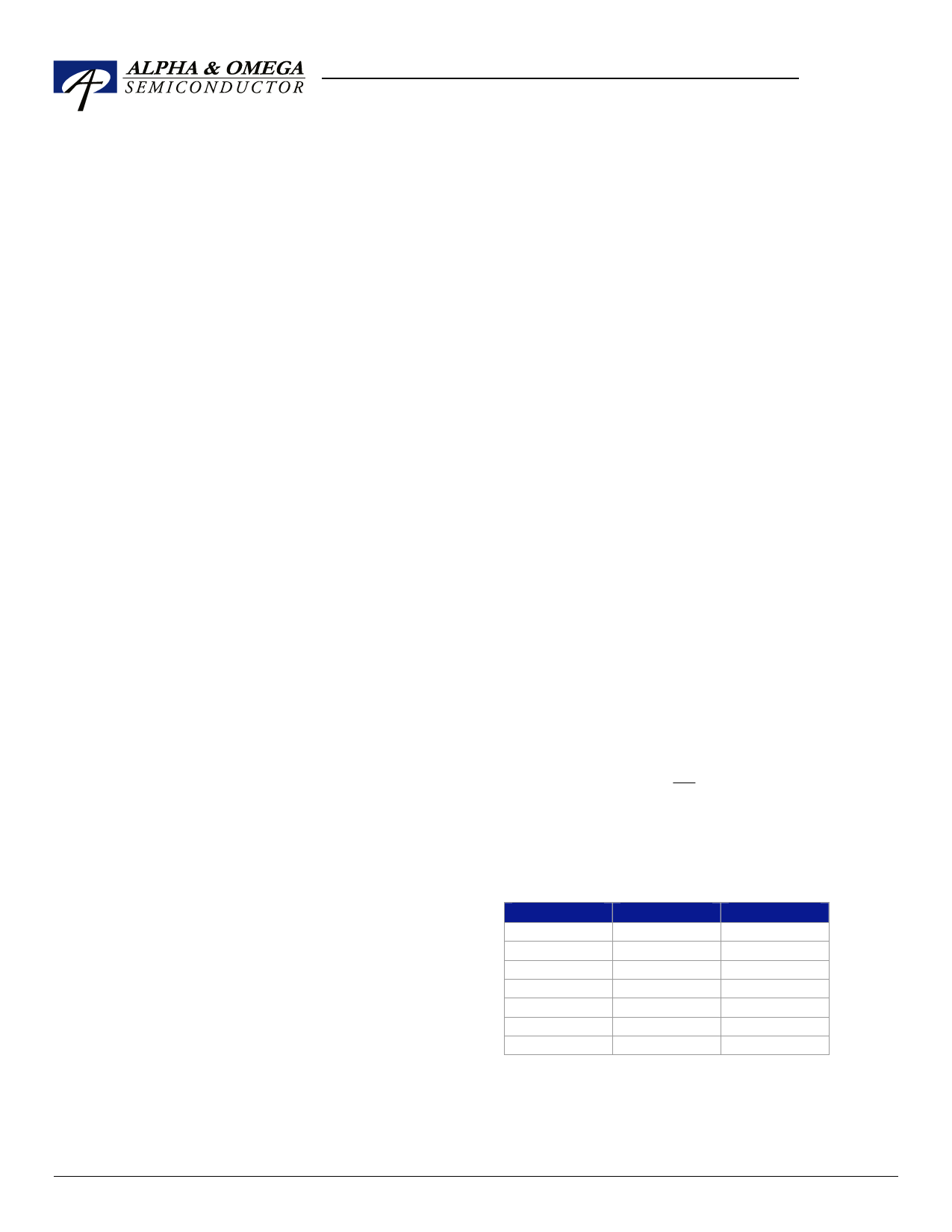
Output Voltage Programming
Output voltage can be set by feeding back the output to
the FB pin with a resistor divider network. In the
application circuit shown in Figure 1. The resistor divider
network includes R1 and R2. Usually, a design is started
by picking a fixed R2 value and calculating the required
R1 with equation below.
VO
=
0.8 × (1 +
R1
R2
)
Some standard value of R1, R2 for most commonly used
output voltage values are listed in Table 1.
Table 1.
Vo (V)
0.8
1.2
1.5
1.8
2.5
3.3
5.0
R1 (kΩ)
1.0
4.99
10
12.7
21.5
31.6
52.3
R2 (kΩ)
open
10
11.5
10.2
10
10
10
Combination of R1 and R2 should be large enough to
avoid drawing excessive current from the output, which
will cause power loss.
February 2006
www.aosmd.com
Page 9 of 21
Share Link: 