PDI1394P11 Ver la hoja de datos (PDF) - Philips Electronics
Número de pieza
componentes Descripción
Lista de partido
PDI1394P11 Datasheet PDF : 20 Pages
| |||
Philips Semiconductors
3-port physical layer interface
Product specification
PDI1394P11
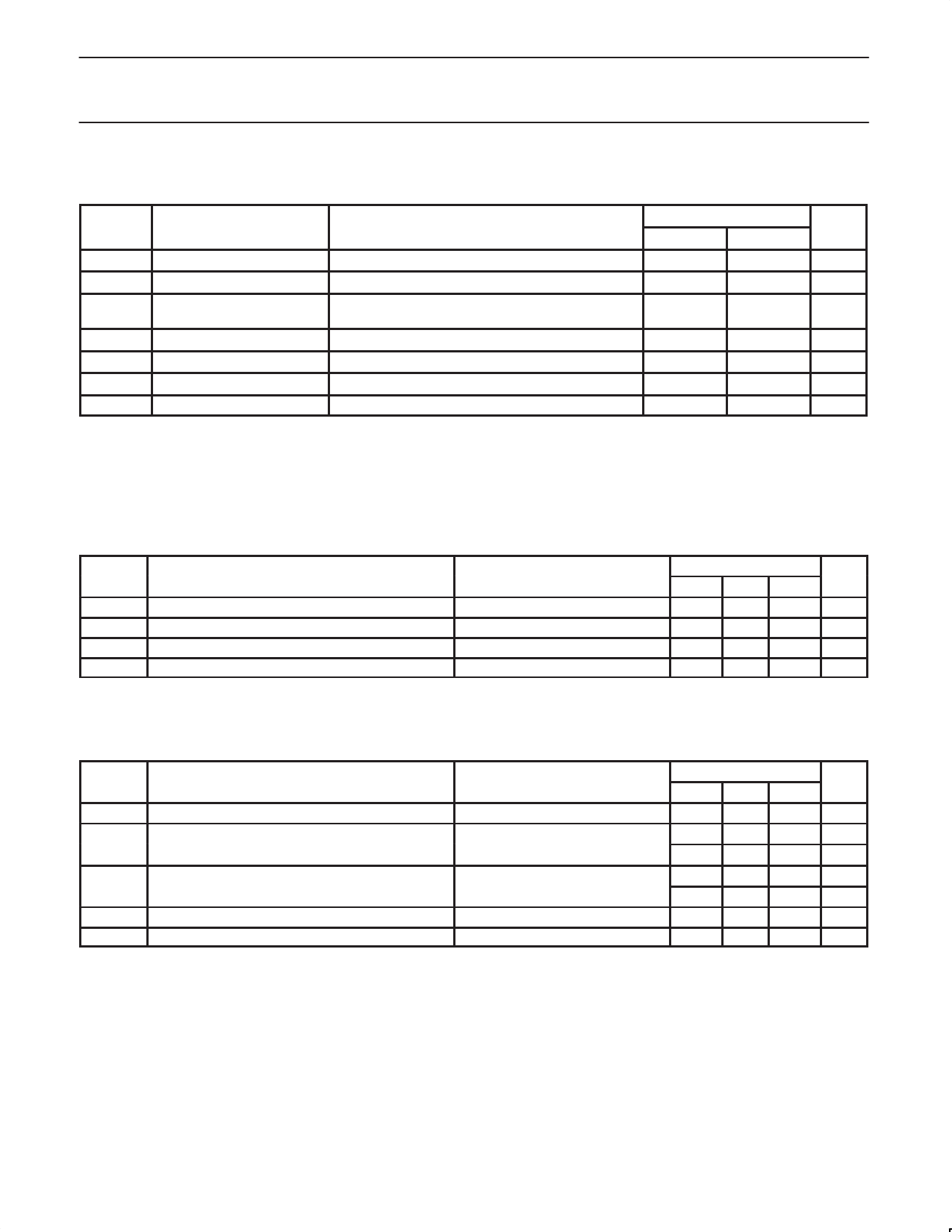
9.0 ABSOLUTE MAXIMUM RATINGS1, 2
In accordance with the Absolute Maximum Rating System (IEC 134). Voltages are referenced to GND (ground = 0V).
SYMBOL
PARAMETER
CONDITION
LIMITS
MIN
MAX
UNIT
VDD
DC supply voltage
–0.3
4.6
V
VI
DC input voltage3
Inputs CPS, TPAn, TPBn, FILTER, XI
–0.5
VDD+0.5
V
VI,5t
DC input voltage
5V tolerant digital inputs RESET–, LPS, LREQ, PD,
CTL[0:1], D[0:3], TESTM[2:1], C/LKON, PC[0:2], ISO–
–0.5
5.5
V
VO
DC output voltage3
–0.5
VDD+0.5
V
IIK
DC input diode current
VI < 0
–
–50
mA
IOK
DC output diode current
VO < 0 or VO > VDD
–
±50
mA
Tstg
Storage temperature range
–65
+150
°C
NOTES:
1. Stresses beyond those listed may cause permanent damage to the device. These are stress ratings only and functional operation of the
device at these or any other conditions beyond those indicated under “recommended operating conditions” is not implied. Exposure to
absolute-maximum-rated conditions for extended periods may affect device reliability.
2. The performance capability of a high-performance integrated circuit in conjunction with its thermal environment can create junction
temperatures which are detrimental to reliability. The maximum junction temperature of this integrated circuit should not exceed 150°C.
3. The input and output voltage ratings may be exceeded if the input and output clamp current ratings are observed.
10.0 CABLE DRIVER
SYMBOL
PARAMETER
TEST CONDITION
LIMITS
UNIT
MIN TYP MAX
VOD
IO(diff)
Differential output voltage
Difference current, TPA+, TPA–, TPB+, TPB–
56 W load
172
Driver enabled, speed signaling OFF –1.051
265 mV
1.051 mA
ISP
Common mode speed signaling current, TPB+, TPB– 200Mbit speed signaling enabled
+2.532
+4.842 mA
VOFF OFF state common mode voltage
Drivers disabled
20
mV
NOTES:
1. Limits defined as algebraic sum of TPA+ and TPA– driver currents. Limits also apply to TPB+ and TPB– algebraic sum of driver currents.
2. Limits defined as one half of the algebraic sum of currents flowing into TPB+ and TPB–.
11.0 CABLE RECEIVER
SYMBOL
PARAMETER
IIC
Common mode input current
ZID
Differential input impedance
ZIC
Common mode input impedance
VTH Receiver input threshold voltage
VTH Cable bias detect threshold, TPBn cable inputs
TEST CONDITION
Driver disabled
Driver disabled
Driver disabled
Driver disabled
LIMITS
MIN TYP MAX
–20
20
15
6
20
24
–60
60
0.6
1.0
UNIT
µA
kΩ
pF
kΩ
pF
mV
V
1999 Apr 09
6
Share Link: 