BD3004HFP Ver la hoja de datos (PDF) - ROHM Semiconductor
Número de pieza
componentes Descripción
Lista de partido
BD3004HFP Datasheet PDF : 9 Pages
| |||
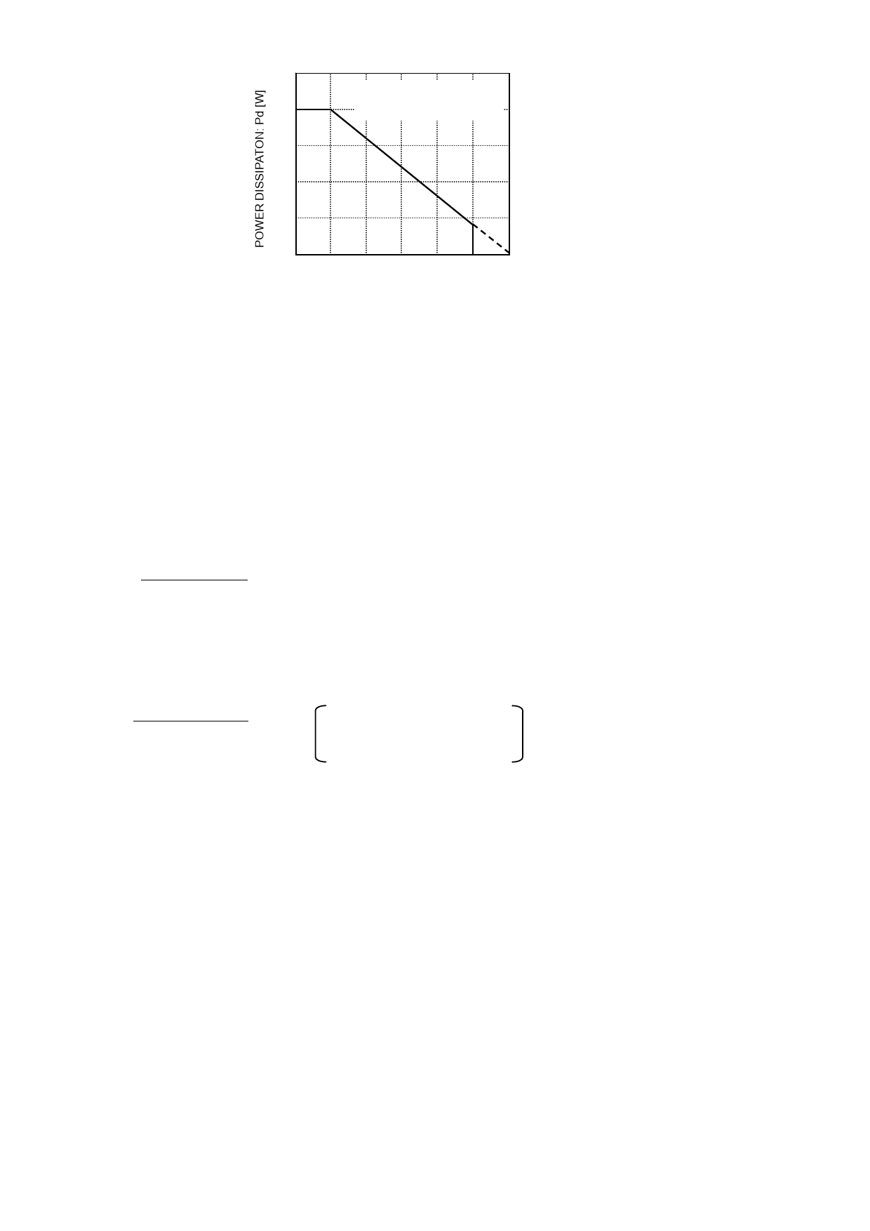
zSetting of heat
2.0
ROHM standard board
Board size: 70 mm × 70 mm × 1.6 mm
1.6
θja = 78.1 (°C /W)
1.2
0.8
0.4
0
0 25 50 75 100 125 150
AMBIENT TEMPERATURE: Ta [℃]
Fig.17
Refer to the dissipation reduction illustrated in Fig.17 when using the IC in an environment where Ta ≥ 25°C. The characteristics of the IC are
greatly influenced by the operating temperature. If the temperature exceeds the maximum junction temperature Tjmax, the elements of the IC
may be damaged. It is necessary to give sufficient consideration to the heat of the IC in view of two points, i.e., the protection of the IC from
instantaneous damage and the maintenance of the reliability of the IC in long-time operation.
In order to protect the IC from thermal destruction, the operating temperature of the IC must not exceed the maximum junction temperature
Tjmax. Fig.17 illustrates the power dissipation/heat mitigation characteristics for the HRP-7 package. Always operate the IC within the power
dissipation (Pd). The following method is used to calculate the power consumption Pc (W).
Pc = (Vcc − VOUT) × IOUT + Vcc × Icc
Power dissipation Pd ≤ Pc
The load current Io is obtained to operate the IC within the power dissipation.
Vcc : Input voltage
VOUT : Output voltage
IOUT : Load current
Icc : Total supply current
IOUT ≤
Pd – Vcc × Icc
Vcc − VOUT
For Icc, see Fig. 1.
From the above, the maximum load current IOUTmax for the applied voltage Vcc can be calculated during the thermal design process.
Calculation example
Example: at Ta = 85°C, Vcc = 12 V, VOUT = 5 V
IOUT≤
0.832 − 12 × Icc
12 − 5
IOUT ≤ 118 mA (Icc = 80 µA)
θja = 78.1°C/W → −12.8 mW/°C
25°C = 1.6 W → 85°C = 0.832 mW
Make a thermal calculation in consideration of the above equations so that the whole operating temperature range will be within the power
dissipation. The power consumption Pc of the IC, in the event of shorting (i.e., if the Vo and GND pins are shorted), will be obtained from the
following equation:
Pc = Vcc × (Icc + Ishort) Ishort = Short current
zExternal settings for pins and precautions
1) Vcc pin
Insert capacitors with a capacitance of 0.33 µF to 1,000 µF between the Vcc and GND pins.
The capacitance varies with the application. Be sure to design the capacitance with a sufficient margin.
2) Output pin
Capacitors for stopping oscillation must be placed between each output pin and the GND pin. Capacitor capacitance values can be
used in a range between 0.1 µF and 1,000 µF. Since oscillation does not occur even for ESR values from 0.001 Ω to 100 Ω, a ceramic
capacitor can be used. Abrupt input voltage and load fluctuations can affect output voltages. Output capacitor capacitance values
should be determined after sufficient testing of the actual application
3) CT pin
Be sure to connect a capacitor to the CT pin. The reset output delay time is given by equation (1) on P. 5. The WDT time is given by
equations (2) and (3) on P.5. The setting times are proportional to the capacitance value of CT pin from the equations, so the maximum
and minimum setting times can be calculated from the electrical characteristics according to the capacitance. Note however that the
electrical characteristics do not include the external capacitor's temperature characteristics. The recommended connection capacity for
the CT pin is 0.001 µF to 22 µF.
6/8
Share Link: 