BS616LV1622TIG70 Ver la hoja de datos (PDF) - Brilliance Semiconductor
Número de pieza
componentes Descripción
Lista de partido
BS616LV1622TIG70 Datasheet PDF : 10 Pages
| |||
BSI
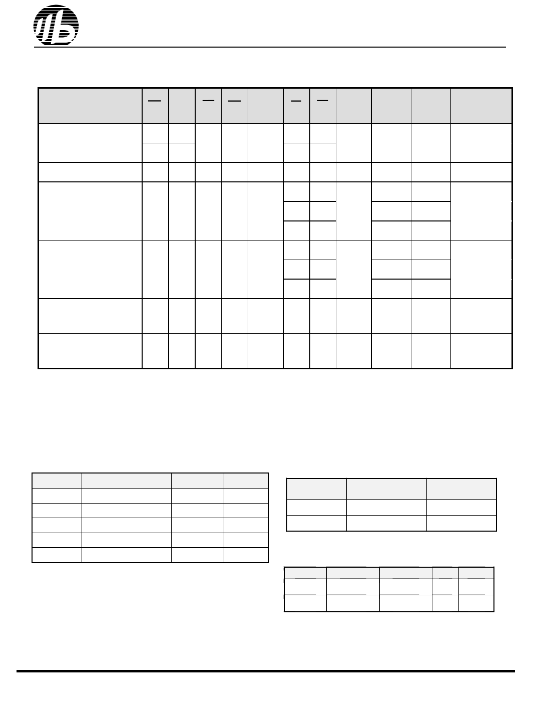
TRUTH TABLE
BS616LV1622
MODE
Fully Standby
Output Disable
Read from SRAM
( WORD mode )
Write to SRAM
( WORD mode )
Read from SRAM
( BYTE Mode )
Write to SRAM
( BYTE Mode )
CE1 CE2 OE WE CIO LB UB SAE D0~7 D8~15 VCC Current
H
X
X
X
X
X
X
X
High-Z High-Z
ICCSB, ICCSB1
X
L
X
X
L
H
H
H
X
X
X
X
High-Z High-Z
ICC
L
H
Dout High-Z
L
H
L
H
H
H
L
X
High-Z Dout
ICC
L
L
Dout
Dout
L
H
Din
X
L
H
X
L
H
H
L
X
X
Din
ICC
L
L
Din
Din
L
H
L
H
L
X
X
A-1
Dout High-Z
ICC
L
H
X
L
L
X
X
A-1
Din
X
ICC
ABSOLUTE MAXIMUM RATINGS(1)
OPERATING RANGE
SYMBOL
VTERM
TBIAS
TSTG
PT
IOUT
PA R A M E T E R
Terminal Voltage with
Respect to GND
Temperature Under Bias
Storage Temperature
Power Dissipation
DC Output Current
R AT IN G
-0.5 to
Vcc+0.5
-40 to +85
-60 to +150
1.0
20
UNITS
V
OC
OC
W
mA
RANGE
Commercial
Industrial
AMBIENT
TEMPERATURE
0 O C to +70 O C
-40 O C to +85 O C
Vcc
2.4V ~ 5.5V
2.4V ~ 5.5V
CAPACITANCE (1) (TA = 25oC, f = 1.0 MHz)
1. Stresses greater than those listed under ABSOLUTE MAXIMUM
RATINGS may cause permanent damage to the device. This is a
stress rating only and functional operation of the device at these
or any other conditions above those indicated in the operational
sections of this specification is not implied. Exposure to absolute
maximum rating conditions for extended periods may affect
reliability.
SYMBOL
CIN
CDQ
PARAMETER
Input
Capacitance
Input/Output
Capacitance
CONDITIONS
VIN=0V
VI/O=0V
MAX.
10
12
UNIT
pF
pF
1. This parameter is guaranteed and not 100% tested.
R0201-BS616LV1622
3
Revision 2.1
Jan. 2004
Share Link: 