BS616LV2017 Ver la hoja de datos (PDF) - Brilliance Semiconductor
Número de pieza
componentes Descripción
Lista de partido
BS616LV2017 Datasheet PDF : 9 Pages
| |||
BSI
BS616LV2017
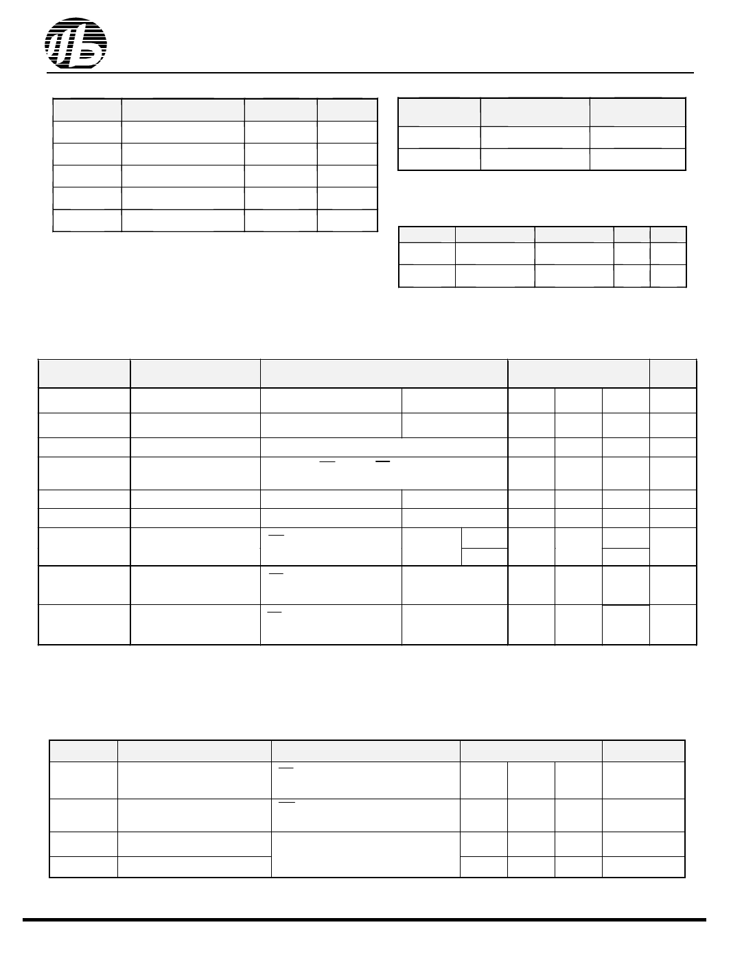
ABSOLUTE MAXIMUM RATINGS(1)
OPERATING RANGE
SYMBOL
V TERM
T BIAS
T STG
PARAMETER
Terminal Voltage with
Respect to GND
Temperature Under Bias
Storage Temperature
RATING
-0.5 to
Vcc+0.5
-40 to +85
-60 to +150
UNITS
V
OC
OC
RANGE
Commercial
Industrial
AMBIENT
TEMPERATURE
0 O C to +70 O C
-40 O C to +85 O C
Vcc
4.5V ~ 5.5V
4.5V ~ 5.5V
PT
I OUT
Power Dissipation
DC Output Current
1.0
W
20
mA
CAPACITANCE (1) (TA = 25oC, f = 1.0 MHz)
SYMBOL PARAMETER CONDITIONS MAX. UNIT
1. Stresses greater than those listed under ABSOLUTE MAXIMUM
RATINGS may cause permanent damage to the device. This is a
stress rating only and functional operation of the device at these
or any other conditions above those indicated in the operational
CIN
CDQ
Input
Capacitance
Input/Output
Capacitance
VIN=0V
VI/O=0V
6 pF
8 pF
sections of this specification is not implied. Exposure to absolute 1. This parameter is guaranteed and not 100% tested.
maximum rating conditions for extended periods may affect
reliability.
DC ELECTRICAL CHARACTERISTICS ( TA = -40 to + 85oC )
PARAMETER
NAME
VIL
VIH
IIL
PARAMETER
TEST CONDITIONS
Guaranteed Input Low
Voltage(2)
Guaranteed Input High
Voltage(2)
Input Leakage Current
Vcc = Max, VIN = 0V to Vcc
Vcc =5.0V
Vcc =5.0V
MIN. TYP. (1) MAX. UNITS
-0.5
--
0.8
V
2.2
--
Vcc+0.3
V
--
--
1
uA
ILO
Output Leakage Current
Vcc = Max,CE = VIH or OE = VIH,
VI/O = 0V to Vcc
--
--
1
uA
VOL
Output Low Voltage
Vcc = Max, IOL = 2.0mA
Vcc =5.0V
--
--
0.4
V
VOH
Output High Voltage
Vcc = Min, IOH = -1.0mA
Vcc =5.0V
2.4
--
--
V
ICC(5)
Operating Power Supply CE = VIL,
Current
IDQ = 0mA, F = Fmax(3)
70ns
Vcc =5.0V
--
55ns
55
--
mA
62
ICCSB
Standby Current-TTL
CE=VIH
IDQ = 0mA
Vcc =5.0V
--
--
1.0
mA
ICCSB1(4)
Standby Current-CMOS
CE≧Vcc-0.2V,
VIN≧Vcc-0.2V or VIN≦0.2V
Vcc =5.0V
--
1.0
30
uA
1. Typical characteristics are at TA = 25oC.
2. These are absolute values with respect to device ground and all overshoots due to system or tester notice are included.
3. Fmax = 1/tRC.
4.IccsB1_Max. is 10uA at Vcc=5.0V and TA=70oC.
5. Icc_Max. is 60mA(@55ns) / 53mA(@70ns) at Vcc=5.0 and TA=0~70oC.
DATA RETENTION CHARACTERISTICS ( TA = -40 to + 85oC )
SYMBOL
PARAMETER
TEST CONDITIONS
VDR
Vcc for Data Retention
CE ≧ Vcc - 0.2V,
VIN ≧ Vcc - 0.2V or VIN ≦ 0.2V
ICCDR (3)
tCDR
tR
Data Retention Current
Chip Deselect to Data
Retention Time
Operation Recovery Time
CE ≧ Vcc - 0.2V,
VIN ≧ Vcc - 0.2V or VIN ≦ 0.2V
See Retention Waveform
1. Vcc = 1.5V, TA = + 25OC
3. IccDR_MAX. is 0.7uA at TA=70oC.
2. tRC = Read Cycle Time
MIN. TYP. (1) MAX.
1.5
--
--
--
0.1
1.0
0
--
--
TRC (2)
--
--
UNITS
V
uA
ns
ns
R0201-BS616LV2017
3
Revision 1.1
Jan. 2004
Share Link: 