PI6C39912 Ver la hoja de datos (PDF) - Pericom Semiconductor Corporation
Número de pieza
componentes Descripción
Lista de partido
PI6C39912
Pericom Semiconductor Corporation

PI6C39912 Datasheet PDF : 11 Pages
| |||
PI6C39911/PI6C39912
3.3V High Speed LVTTL or Balanced Output
11223344556677889900112233445566778899001122334455667788990011221122334455667788990011223344556677889900112233445566778899001122112233445566778899001122P3344r5566o77g8899r00a1122m3344m556677a88b9900l11e2211S2233k44e5566w7788C990011l22o33c44k556677B8899u0011f22f33e44r5566-7788S99u0011p2211e22r33C4455l66o7788c99k0011®22
Test Mode
The TEST input is a three-level input. In normal system operation,
this pin is connected to ground, allowing the PI6C39911 to operate
as explained briefly above (for testing purposes, any of the three
level inputs can have a removable jumper to ground, or be tied LOW
through a 100 Ohm resistor. This will allow an external tester to
change the state of these pins.)
If the TEST input is forced to its MID or HIGH state, the device will
operate with its internal phase locked loop disconnected, and input
levels supplied to REF will directly control all outputs. Relative
output to output functions are the same as in normal mode.
In contrast with normal operation (TEST tied LOW). All outputs
will function based only on the connection of their own function
select inputs (xF0 and xF1) and the waveform characteristics of the
REF input.
Maximum Ratings
Storage Temperature ..................................... 65°C to +150°C
Ambient Temperature with
Power Applied ............................................... 55°C to +125°C
Supply Voltage to Ground Potential ................ 0.5V to +5.0V
DC Input Voltage .............................................. 0.5Vto+5.0V
Output Current into Outputs (LOW) .............................. 64mA
Static Discharge Voltage ............................................... >2001V
(per MIL-STD-883, Method 3015)
Latch-Up Current .........................................................>200mA
Maximum Power Dissipation at TA=85°C(23) ............... 0.80watts
Operating Range
Range
Ambient Temperature
Commercial
0°C to +70°C
Industrial
40°C to +85°C
VCC
3.3V ±10%
3.3V ±10%
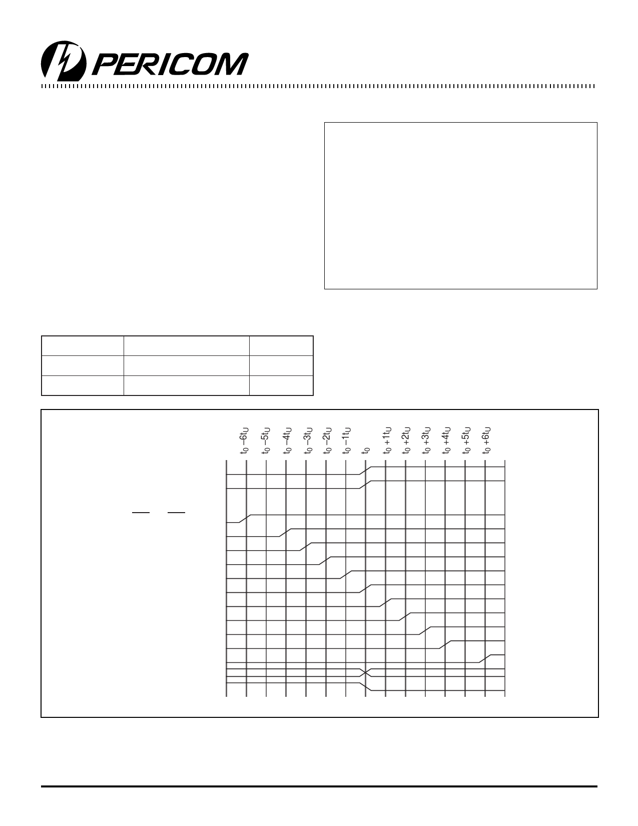
FB Input
REF Input
1Fx 3Fx
2Fx 4Fx
(N/A) LM –6tU
LL LH –4tU
LM (N/A) –3tU
LH ML –2tU
ML (N/A) –1tU
MM MM
0tU
MH (N/A) +1tU
HL MH +2tU
HM (N/A) +3tU
HH HL +4tU
(N/A) HM +6tU
(N/A) LL/HH Divided
(N/A) HH Invert
Figure 1. Typical Outputs with FB Connected to a Zero-Skew Output(3)
Note:
3. FB connected to an output selected for zero skew (i.e., xF1 = xF0 = MID)
3
PS8497A 04/10/01
Share Link: