CY7C185-20PXC Ver la hoja de datos (PDF) - Cypress Semiconductor
Número de pieza
componentes Descripción
Lista de partido
CY7C185-20PXC Datasheet PDF : 15 Pages
| |||
CY7C185
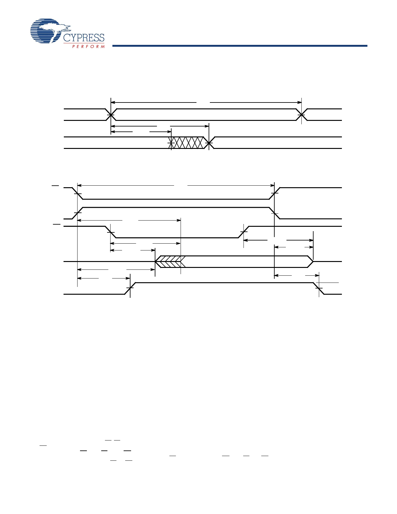
Switching Waveforms
Figure 2. Read Cycle No.1[8,9]
ADDRESS
DATA OUT
tRC
tAA
tOHA
PREVIOUS DATA VALID
Figure 3. Read Cycle No.2[10,11]
CE1
tRC
DATA VALID
CE2
OOEE
DATA OUT
VCC
SUPPLY
CURRENT
tACE
tDOE
tLZOE
HIGH IMPEDANCE
tLZCE
tPU
50%
DATA VALID
tHZOE
tHZCE
HIGH
IMPEDANCE
tPD
ICC
50%
ISB
Notes
8. Device is continuously selected. OE, CE1 = VIL. CE2 = VIH.
9. WE is HIGH for read cycle.
10. Data I/O is High Z if OE = VIH, CE1 = VIH, WE = VIL, or CE2=VIL.
11. The internal write time of the memory is defined by the overlap of CE1 LOW, CE2 HIGH and WE LOW. CE1 and WE must be LOW and CE2 must be HIGH to initiate
write. A write can be terminated by CE1 or WE going HIGH or CE2 going LOW. The data input setup and hold timing must be referenced to the rising edge of the
signal that terminates the write.
Document #: 38-05043 Rev. *E
Page 6 of 15
[+] Feedback
Share Link: 