DS2167 Ver la hoja de datos (PDF) - Dallas Semiconductor -> Maxim Integrated
Número de pieza
componentes Descripción
Lista de partido
DS2167 Datasheet PDF : 15 Pages
| |||
DS2167/DS2168
PRODUCT OVERVIEW
The DS2167 and DS2168 contain three major function-
al blocks: a high performance (10 MIPS) DSP “engine,”
two independent PCM data interfaces (“X” and “Y”)
which connect directly to serial time division multiplexed
(TDM) backplanes and a microcontroller-compatible
serial port for on-the-fly device configuration. A 10MHz
master clock is required by the DSP engine. The de-
vices’ dual channel architecture supports full duplex,
dual compression or dual expansion operation. The
PCM data interfaces support 1.544, 2.048 and 4.096
MHz data rates. Each device samples the serial PCM or
ADPCM bit stream during a user-programmed input
timeslot, processes the data and outputs the result dur-
ing a user-programmed output timeslot.
Each PCM interface has a control register which speci-
fies functional characteristics (compress, expand, by-
pass and idle), data format (µ-law or A-law) and algo-
rithm reset control. With the SPS pin strapped high, the
software mode is enabled and the serial port is used to
program control and timeslot registers. In this mode, a
novel addressing scheme allows multiple devices to
share a common 3-wire control bus, simplifying system
level interconnect.
With SPS low, the hardware mode is enabled. This
mode disables the serial port and maps appropriate
control register bits to address and port inputs. Under
hardware mode, no host controller is required and all
PCM I/O defaults to timeslot 0. This stand-alone mode is
compatible with popular codecs.
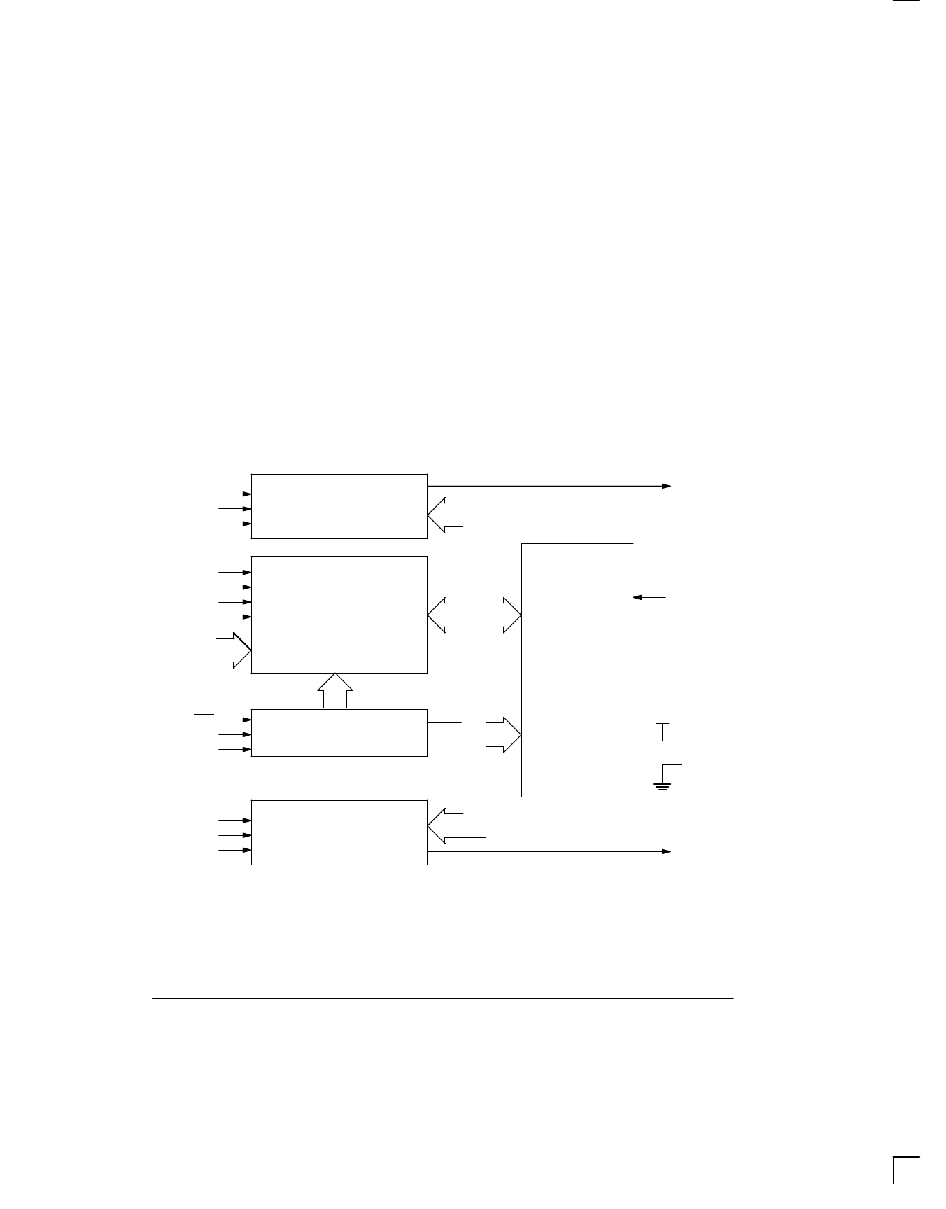
DS2168 BLOCK DIAGRAM Figure 1
FSX
CLKX
XIN
“X” SIDE PCM/ADPCM
DATA INTERFACE
XOUT
SCLK
SPS
CS
SDI
A0 - A5
SERIAL PORT CONTROL/
HARDWARE MODE LOGIC
ADPCM
PROCESSING
“ENGINE”
MCLK
RST
TM0
TM1
RESET AND TEST LOGIC
VDD
VSS
FSY
CLKY
YIN
“Y” SIDE PCM/ADPCM
DATA INTERFACE
YOUT
022698 2/15
Share Link: 