RF2162 Ver la hoja de datos (PDF) - RF Micro Devices
Número de pieza
componentes Descripción
Lista de partido
RF2162 Datasheet PDF : 10 Pages
| |||
RF2162
Preliminary
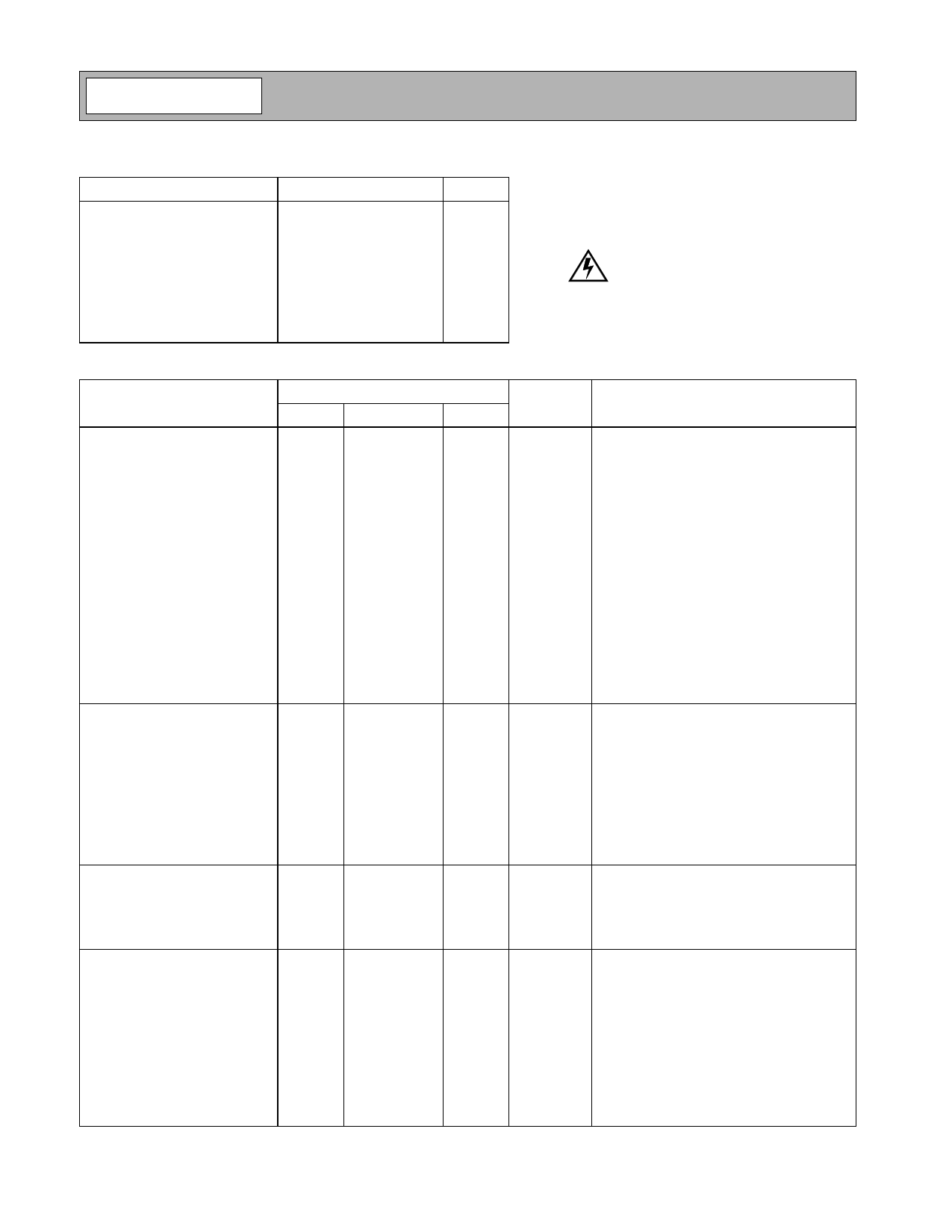
Absolute Maximum Ratings
Parameter
Rating
Supply Voltage (RF off)
+8.0
Supply Voltage (POUT≤31dBm)
Mode Voltage (VMODE)
Control Voltage (VPD)
Input RF Power
Operating Case Temperature
Storage Temperature
Moisture Sensitivity
+4.5
+3.0
+3.0
+12
-30 to +110
-30 to +150
Modified JEDEC Level 2
Unit
VDC
VDC
VDC
VDC
dBm
°C
°C
Caution! ESD sensitive device.
RF Micro Devices believes the furnished information is correct and accurate
at the time of this printing. However, RF Micro Devices reserves the right to
make changes to its products without notice. RF Micro Devices does not
assume responsibility for the use of the described product(s).
Parameter
Overall
Usable Frequency Range
Typical Frequency Range
Linear Gain
Second Harmonic (including
second harmonic trap)
Max CW Output Power
Total Efficiency (AMPS mode)
Maximum Linear Output Power
(CDMA Modulation)
Total Linear Efficiency
Adjacent Channel Power Rejec-
tion
Noise Power
Maximum Linear Output Power
(CDMA Modulation)
Total Efficiency (AMPS mode)
Max CW Output Power
Total Linear Efficiency
Adjacent Channel Power Rejec-
tion
Input VSWR
Output Load VSWR
TDMA
Linear Output Power
Linear ACP
Linear ALT CP
Efficiency
Power Supply
Power Supply Voltage
Idle Current
VREG Current
Turn On/Off time
Total Current (Power down)
VREG “Low” Voltage
VREG “High” Voltage
VMODE Bias Control Voltage
Range
Specification
Min.
Typ.
Max.
800
960
824-849
28
29
31
-30
31.5
50
29
30
35
-46
-44
-58
-56
-90
-89
29
50
30
30.5
31
30
36
-46
-44
-58
-56
< 2:1
10:1
30
-29
-28
-49
-48
45
46
3.0
3.4
4.5
135
200
10
15
<100
10
0
0.2
2.7
2.8
2.9
0 to 2.5
Unit
MHz
MHz
dB
dBc
dBm
%
dBm
%
dBc
dBc
dBm
dBm
%
dBm
%
dBc
dBc
dBm
V
mA
mA
ns
μA
V
V
V
Condition
T=25°C, VCC=3.4V, Freq=824MHz to
849MHz unless otherwise specified
ACPR @ 885kHz
ACPR @1980kHz
VCC=3.4V; BW=30kHz; RX Band NF mea-
sure from TX center band to RX center band.
VCC = 3.0 V
ACPR @ 885kHz
ACPR @ 1980kHz
No damage.
30kHZ offset
60kHZ offset
O/P = 30 dBm
VMODE=0V to 0.5V
Total pins 6 and 7, VREG=2.8V
VPD = Low
2-228
Rev A19 060208
Share Link: 