RF2627PCBA Ver la hoja de datos (PDF) - RF Micro Devices
Número de pieza
componentes Descripción
Lista de partido
RF2627PCBA Datasheet PDF : 6 Pages
| |||
RF2627
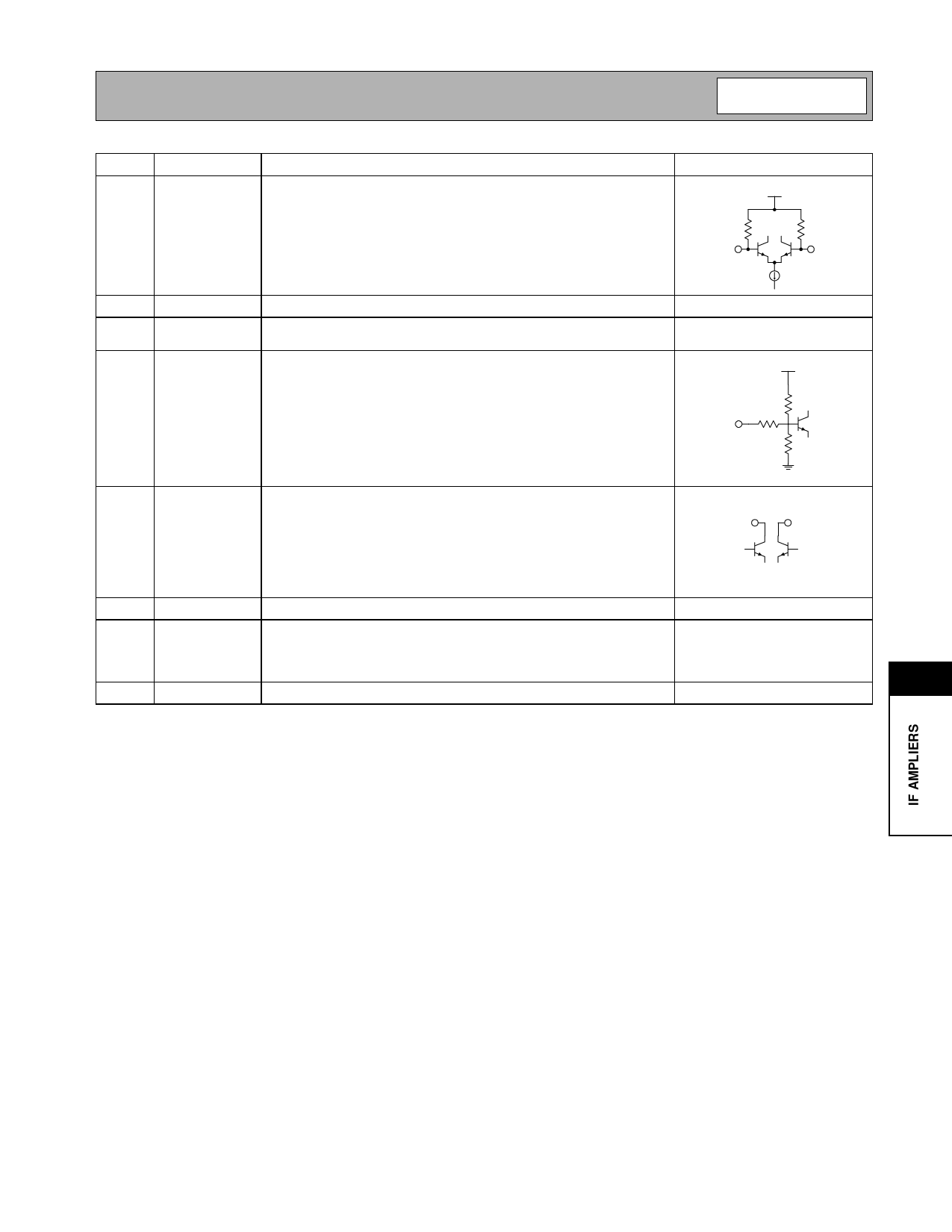
Pin
1
2
3
4
Function
IN+
Description
CDMA Balanced Input Pin. This pin is internally DC biased and should
be DC blocked if connected to a device with a DC level other than VCC
present. A DC to connection to VCC is acceptable. For single-ended
input operation, one pin is used as an input and the other CDMA input
is AC coupled to ground. The balanced input impedance is 1kΩ, while
the single-ended input impedance is 500Ω.
Interface Schematic
BIAS
CDMA+
700 Ω
700 Ω
CDMA-
IN-
GND
GC
Same as pin 2, except complementary input.
Ground connection. Keep traces physically short and connect immedi-
ately to ground plane for best performance.
Analog gain adjustment for all amplifiers. Valid control ranges are from
0V to 3.0V. Maximum gain is selected with 3.0V. Minimum gain is
selected with 0V. These voltages are only valid for a 4.7kΩ DC source
impedance.
See pin 1.
VCC
12.7 kΩ
23.5 kΩ
15 kΩ
5
OUT-
Balanced Output pin. This is an open-collector output, designed to
operate into a 250Ω balanced load. The load sets the operating imped-
ance, but an external choke or matching inductor to VCC must also be
OUT+
OUT-
supplied in order to correctly bias this output. This bias inductor is typi-
cally incorporated in the matching network between the output and next
stage. Because this pin is biased to VCC, a DC blocking capacitor must
be used if the next stage’s input has a DC path to ground.
6
OUT+
Same as pin 5, except complementary output.
See pin 5.
7
VCC1
Supply Voltage pin. External bypassing is required. The trace length
between the pin and the bypass capacitors should be minimized. The
ground side of the bypass capacitors should connect immediately to
ground plane.
8
VCC2
Same as pin 7.
10
Rev A8 010711
10-35
Share Link: 