RF2627PCBA Ver la hoja de datos (PDF) - RF Micro Devices
Número de pieza
componentes Descripción
Lista de partido
RF2627PCBA Datasheet PDF : 6 Pages
| |||
RF2627
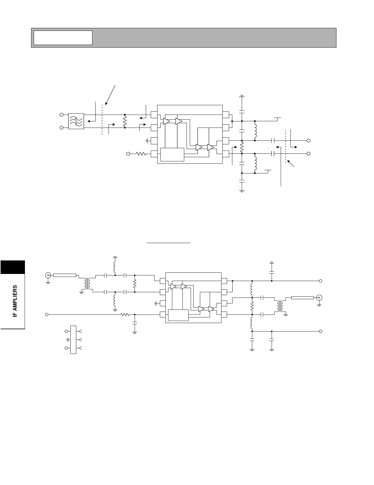
Application Schematic
Measurement
Reference Plane
ZS=500 Ω
CDMA IF Filter
CDMA+
CDMA-
Z IN, EFF=500 Ω
Z S, EFF=333 Ω
1
R1:
1 kΩ
2
Z IN=1 kΩ
3
GAIN
4
GAIN
4.7 kΩ
CONTROL
8
7
6
5
ZLOAD,EFF=250 Ω
R1 sets the CDMA balanced input impedance. The effective input impedance is then 500 Ω.
R2 sets the balanced output impedance to 500 Ω. L1 and C2 serve dual purposes. L1 serves
as an output bias choke, and C2 serves as a series DC block. In addition, the values of L1
and C2 may be chosen to form an impedance matching network of the load impedance is not
500 Ω. Otherwise, the values of L1 and C1 are chosen to form a parallel-resonant tank circuit
at the IF when the load impedance is 500 Ω.
10 nF
VCC
C1 L1
C2
R2: 500Ω C2
ZLOAD=500Ω
OUT+
OUT-
C1 L1
VCC
Measurement
Reference Plane
10 nF
ZOUT=500 Ω
Evaluation Board Schematic
(Download Bill of Materials from www.rfmd.com.)
10
CDMA
J1
SMA
50 Ω µstrip
T1
GC
P1
P1-1 1 VCC
2 GND
P1-3 3
GC
C3
15 pF
L1
390 nH
C4
15 pF
C1
10 nF
R1
1 kΩ
L2
390 nH
C2
10 nF
R2
4.7 kΩ
C5
1 nF
1
2
3
4
GAIN
CONTROL
2627400A
C10
10 nF
8
VCC
L4
C8
7
390nH 15 pF
OUT
J2
6
R3
T2
50 Ω µstrip
SMA
510 Ω
5
L3
390nH
C9
15 pF
VCC
C6
10 nF
C7
10 nF
10-36
Rev A8 010711
Share Link: 