TQ5132 Ver la hoja de datos (PDF) - TriQuint Semiconductor
Número de pieza
componentes Descripción
Lista de partido
TQ5132 Datasheet PDF : 12 Pages
| |||
TQ5132 Product Description
The TQ5132 is a miniature low noise mixer (downconverter) in a
small SOT-23-8 package (2.9X2.8X1.14 mm) with operation at
2.8v. The TQ5132 specs are designed to be compatible with IS-
98 Interim Standard for Dual-Mode CDMA cellular systems. The
low noise mixer features an AMPS control pin for Gain, Intercept
and Current (GIC pin) and it has excellent intermodulation
characteristics with high intercept point in all modes. For
optimum performance the TQ5132 RF frequency of operation
should be from 869 to 894 MHz. The IF range is from 85 to 130
MHz and its injection mode for the local oscillator is high side.
Operation
The TQ5132 is a single-ended mixer with switching capabilities
for the various signal levels found in CDMA applications. The
TQ5132 combines a RF amplifier, a LO driver amplifier, and
separate digitally controlled IF amplifiers for CDMA and AMPS
outputs.
RF / C2 1
TQ5132
8 Mx Vdd
GND 2
7 LO / C1
GIC 3
6 IFA GS / C3
CDMA
IF
4
Output
AMPS
5 IF
Output
Figure 1. TQ5132 Block Diagram
Circuit Description
RF Amplifier
The TQ5132 has an integrated pre-amplifier stage in a cascode
configuration. The output is internally matched to 50 ohms at
881MHz. Pin 1 requires an external match that is set to deliver a
2:1 VSWR in both the low and high gain modes (i.e. RFA is on
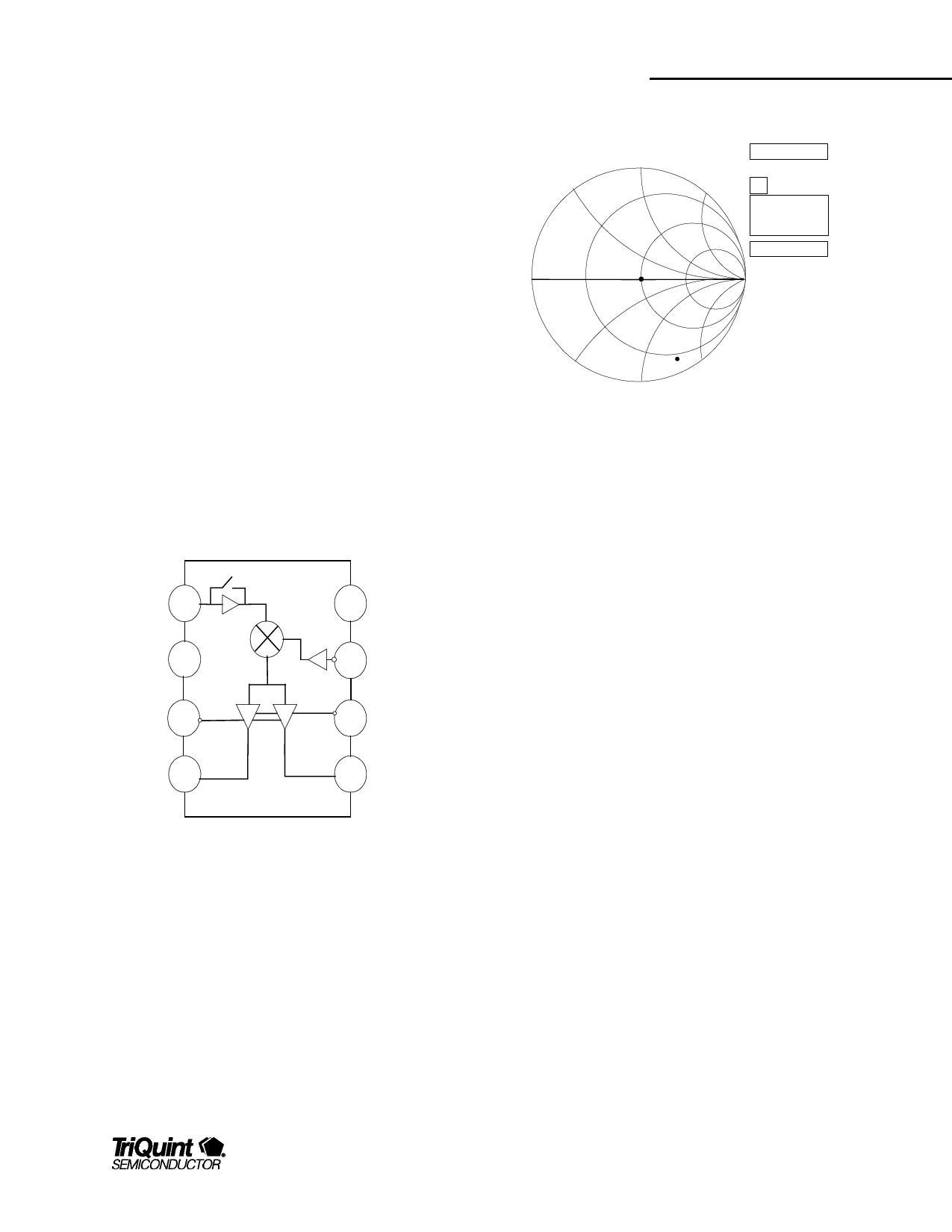
or off). Figure 2 shows an approximated impedance at pin 1
(RFA input) to implement any desired match. Remember to
apply the LO signal when tuning the RF match.
TQ5132
Data Sheet
0.5
0.5
1.0
2.0
1.0
2.0
TQ5132
Input
A Impedance
0.76 @ -65.5
z = 0.44 - j 1.46
y = 0.19 + j 0.63
Freq=881MHz
A
-0.5
-2.0
-1.0
Figure 2. TQ5132 RF Amplifier Input Impedance
LO Buffer Amplifier
The LO buffer amplifier is a grounded gate FET with a
broadband match to 50Ω. It has on-chip DC block and on-chip
LO tuning circuit to shape the frequency response and drive it to
a level suitable for the gate of the mixer FET. Thus the optimum
LO frequency range is fixed and centered around 990mhz. The
LO is limited to high-side injection mode and it operates from
950MHz to 1030MHz. The input to the LO buffer is through pin 7
which also feeds the control line (C1) that selects the mixer
mode of operation, either CDMA or AMPS. Due to this logic
control, the only external component required at the LO port is a
series capacitor to prevent DC from traveling to other parts of
the system. The LO drive level of operation should be between -
7 and 0 dBm. Best performance is obtained between –6 and –
2 dBm.
LO/filter/Mixer interaction
The physical position of the image reject filter is likely to have an
effect on the performance of the mixer especially in the Low
Gain mode where the RF amplifier is switched out. This is
primarily due to self-mixing of the LO energy bouncing from the
filter back into the mixer either out-of-phase or in-phase creating
an offset in magnitude. To minimize this effect, TriQuint
recommends placing the image-reject filter as close to the IC as
possible. In TriQuint’s demo board its position is 42 mils from
the pad of the matching inductor and 126 mils from the IC pad.
This location for the image-reject filter works well.
For additional information and latest specifications, see our website: www.triquint.com
7
Share Link: 