TQ5132 Ver la hoja de datos (PDF) - TriQuint Semiconductor
Número de pieza
componentes Descripción
Lista de partido
TQ5132 Datasheet PDF : 12 Pages
| |||
of the IF match should be grounded close to the IC (see figure
6).
After designing the IF match in simulation using the given S-
parameters, some adjustment might be needed when
implementing the match on the bench. At this point remember
that the LO driver amplifier must be turned on since the IFA is
directly coupled to the mixer FET. Figure 6 shows the circuit
topology and component values designed for TriQuint's demo
board. Figure 7 shows a typical AMPS IF output impedance.
TQ5132
1
8
2
7
3
6
C9=15pF
4
5
L3=270nH
C10=18pF
AMPS
IF
Output
Vdd
Note: These values were optimized for TriQuint's 5131 Demo
board. The discrepancy between these values and those of the
customer's application may differ due to board and component
parasitics.
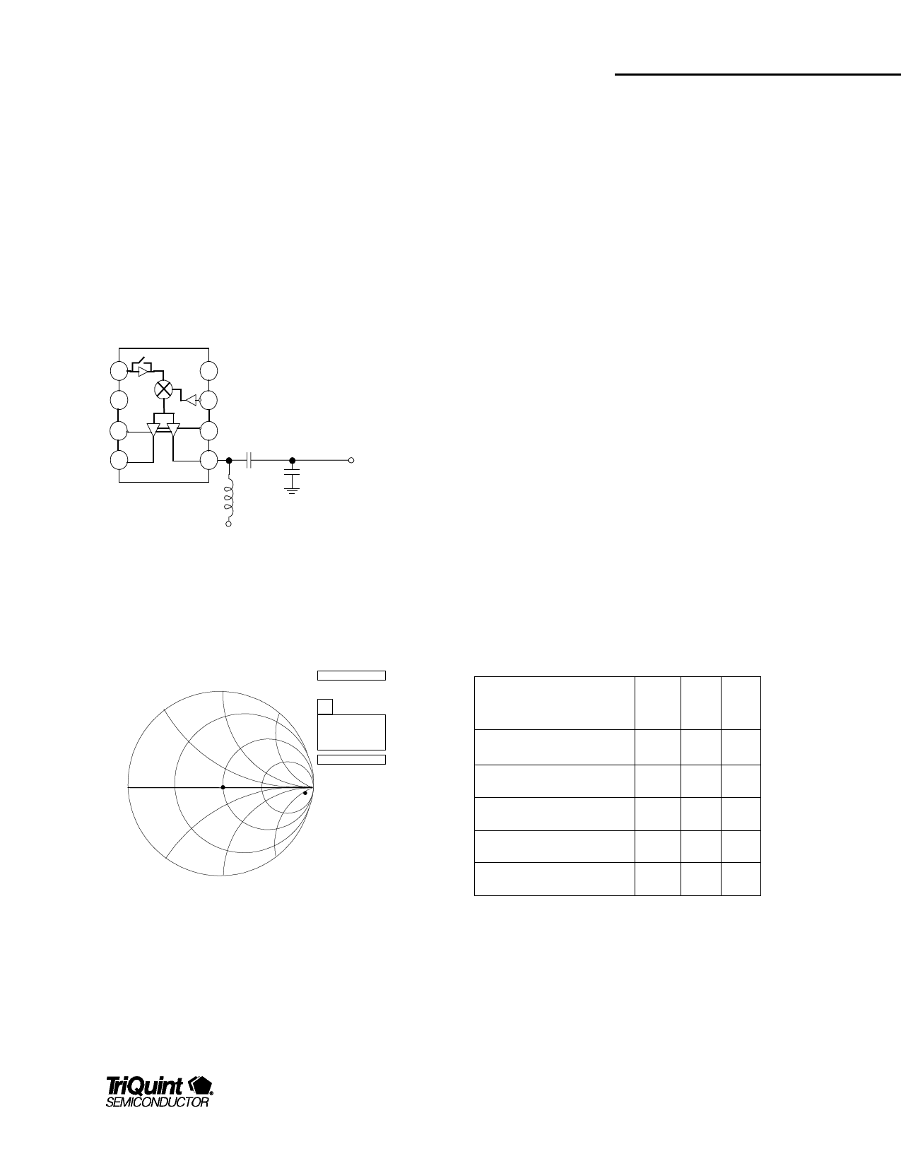
Figure 6. TQ5132 AMPS IF Output Match (IF = 85 MHz)
0.5
0.5
1.0
1.0
2.0
TQ5132
AMIF output
2.0
C Impedance
0.9 @ - 2.9
z = 15.4 - j 7.23
y = 0.05 + j 0.02
Freq=85MHz
C
-0.5
-2.0
-1.0
Figure 7. TQ5132 AMPS IF Output Impedance at Pin 5
Vdd Decoupling
External spurious signals at high and low frequencies can
appear on the Vdd lines. Proper decoupling of these lines is
required to eliminate unwanted noise. The recommended
TQ5132
Data Sheet
decoupling network has a PI configuration. On the main Vdd
node, a large capacitor of 0.022 uF is used, followed by a 3.3 or
10 ohm resistor in series with the supply line. Last, a bypass
capacitor that presents a low impedance to ground at the RF
frequency is normally placed very close to the pin. However, in
the TQ5132 this bypass capacitor on the IC node is on-chip and
the external one near the IC is not needed.
Board Layout Recommendations
All ground pins should be kept close to the IC and have its own
via to the ground plane to minimize inductance.
Most PC boards for portable applications have thin dielectric
layers and very narrow line width which increase the board
parasitic capacitance and inductance. To minimize these effects
when implementing a matching network, it is recommended to
relieve the ground underneath pads carrying RF signals
whenever possible.
Control Line Description
The control lines can be toggled between high and low levels
using CMOS logic circuitry. Control line C1 is used to switch
between CDMA and AMPS IF output. The other two control
lines C2 and C3 set the various CDMA output levels required by
the system.
Table 1. Downconverter Control Lines C1, C2, C3
Receiver State
C1 C2 C3
AMPS Mode
0
01
CDMA High Gain
1
00
CDMA HG, low lin
1
01
CDMA Mid Gain
CDMA Low Gain
1
10
1
11
C1 = Mixer Mode, C2 = RFA gain select and LNA gain select,
C3 = IFA gain select and LNA mode select.
For additional information and latest specifications, see our website: www.triquint.com
9
Share Link: 