RF2161 Ver la hoja de datos (PDF) - RF Micro Devices
Número de pieza
componentes Descripción
Lista de partido
RF2161 Datasheet PDF : 8 Pages
| |||
RF2161
Preliminary
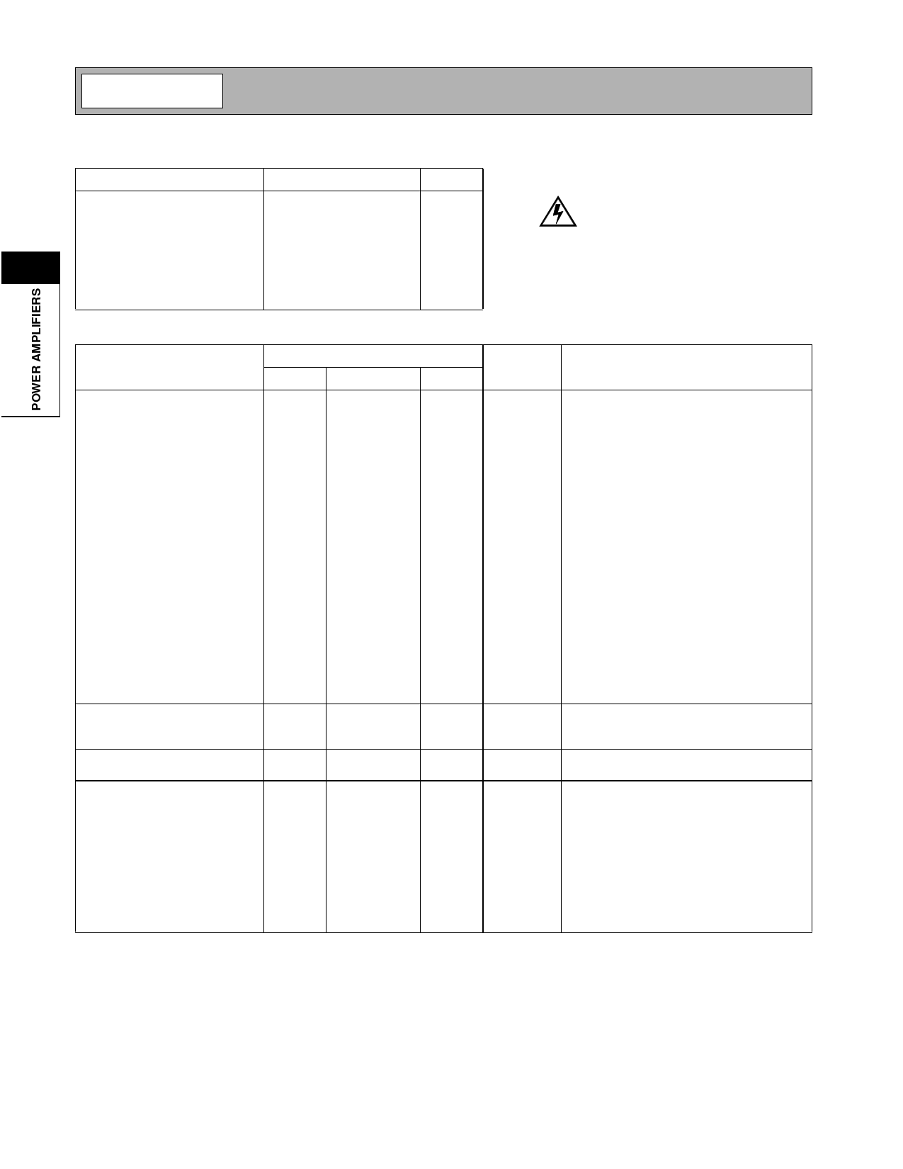
Absolute Maximum Ratings
Parameter
Rating
Supply Voltage (RF off)
+8.0
Supply Voltage (POUT≤31dBm)
Mode Voltage (VMODE)
2
Control Voltage (VPD)
Input RF Power
Operating Case Temperature
Storage Temperature
+5.0
+3.0
+3.0
+6
-30 to +100
-30 to +150
Unit
VDC
VDC
VDC
VDC
dBm
°C
°C
Caution! ESD sensitive device.
RF Micro Devices believes the furnished information is correct and accurate
at the time of this printing. However, RF Micro Devices reserves the right to
make changes to its products without notice. RF Micro Devices does not
assume responsibility for the use of the described product(s).
Parameter
Overall
Usable Frequency Range
Typical Frequency Range
Linear Gain
Second Harmonic (including
second harmonic trap)
Third Harmonic
Fourth Harmonic
Maximum Linear Output Power
(W-CDMA Modulation)
Total Linear Efficiency
Adjacent Channel Power
Rejection @ 5 MHz
Adjacent Channel Power
Rejection @ 10MHz
Noise Power
Maximum Linear Output Power
(W-CDMA Modulation)
Total Linear Efficiency
Input VSWR
Output Load VSWR
Power Supply
Power Supply Voltage
Idle Current
VPD Current
Total Current (Power down)
VPD “Low” Voltage
VPD “High” Voltage
MODE “High” Voltage
MODE “Low” Voltage
Specification
Min.
Typ.
Max.
1850
28
26
27
30
3.0
2.7
2.5
1850 to 1910
1920 to 1980
30
28
-35
-40
-45
35
-40
-50
-137
26
35
< 2:1
3.4
120
13
10
0
2.8
2.8
0
2000
-38
-48
5:1
5.0
10
0.2
2.9
0.5
Unit
MHz
MHz
Condition
T=25 °C, VCC=3.4V unless otherwise speci-
fied
dB
dB
dBc
dBc
dBc
dBm
%
dBc
dBc
dBm/Hz
dBm
%
Mode = Low
Mode = High
VMODE High, POUT=27dBm
POUT=27dBm, W-CDMA Modulation
3G PP 3.2 03-00 DPCCH+1DPDCH
POUT=27dBm, W-CDMA Modulation
3G PP 3.2 03-00 DPCCH+1DPDCH
POUT=+27dBm, Rx Band 2110MHz to
2170 MHz
VCC = 3.0 V
No oscillations
V
mA
MODE = high
mA
Total pins 6 and 8, VPD = 2.8 V
µA
VPD = low
V
V
2-198
Rev A3 010514
Share Link: 