RF2161 Ver la hoja de datos (PDF) - RF Micro Devices
Número de pieza
componentes Descripción
Lista de partido
RF2161 Datasheet PDF : 8 Pages
| |||

Preliminary
RF2161
Pin Function Description
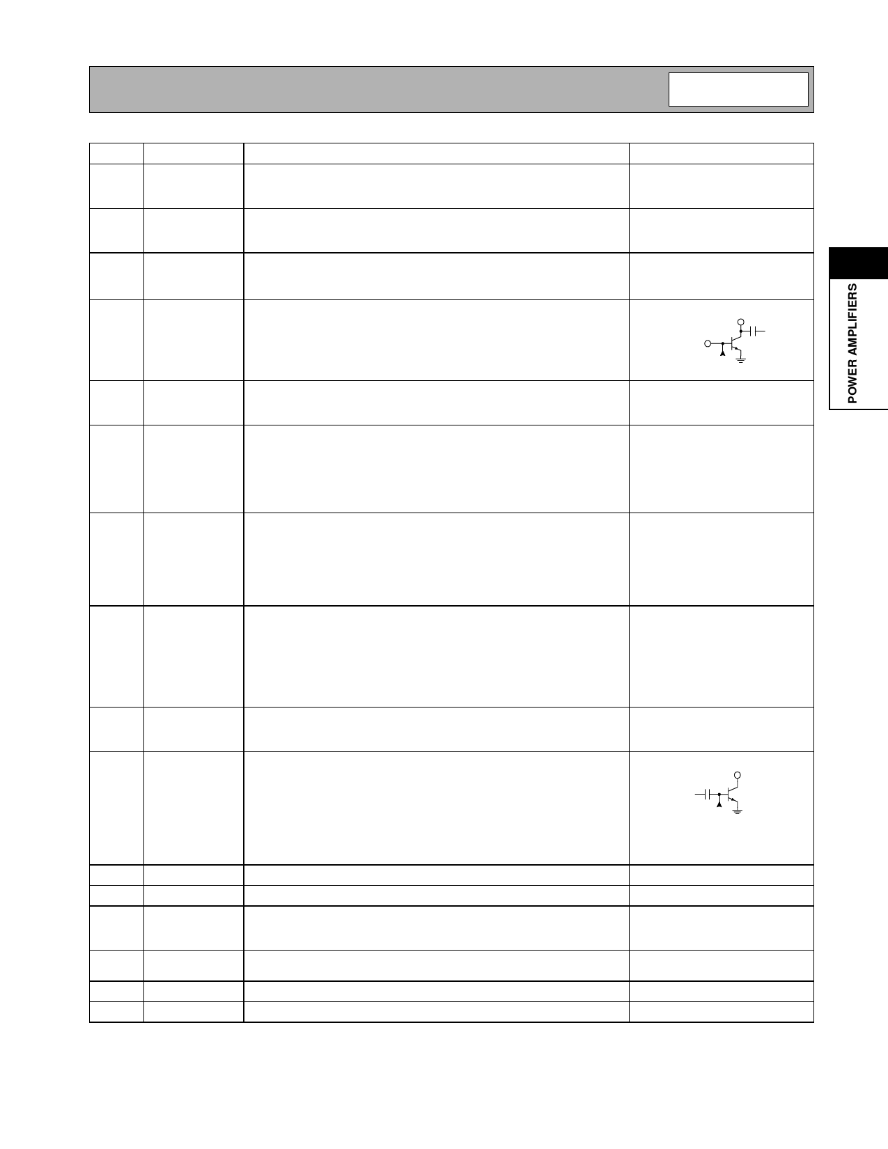
Interface Schematic
1
VCC2
Power supply for second stage and interstage match. Pins 1, 15 and 16
should be connected by a common trace where the pins contact the
printed circuit board.
2
GND2
Ground for second stage. For best performance, keep traces physically
short and connect immediately to ground plane. This ground should be
isolated from the backside ground contact.
3
VCC1
Power supply for first stage and interstage match. VCC should be fed See pin 4.
2
through a 1.2nH inductor terminated with a 8.2pF capacitor on the sup-
ply side. The inductor should be as close to the pin as possible.
4
RF IN
RF input. An external series capacitor is required as a DC block. The
input match can be improved to <2:1 by using a series capacitor and
shunt inductor.
VCC1
RF IN
From Bias
Stages GND1
5
GND1
Ground for first stage. For best performance, keep traces physically See pin 4.
short and connect immediately to ground plane. This ground should be
isolated from the backside ground contact.
6
VPD1
Power Down control for first and second stages. When this pin is “low”,
all first and second stage circuits are shut off. When this pin is 2.8V, all
first and second stage circuits operate normally. VPD1 requires a regu-
lated 2.8V for the amplifier to operate properly over all specified tem-
perature and voltage ranges. A dropping resistor from a higher
regulated voltage may be used to provide the required 2.8V.
7
VMODE VMODE adjusts the bias to the 2nd and 3rd stages. For full power oper-
ation, MODE is set low. When operating in a lower output power mode
(<+25dBm) this pin is set high to reduce bias current by up to 50%. An
external series resistor is optional to limit the amount of current
required. At low temperature (-30οC), it is recommended to set VMODE
low to maintain correct operation.
8
VPD2
Power Down control for third stage. When this pin is “low”, all and third
stage circuits are shut off. When this pin is 2.8V, all and third stage cir-
cuits operate normally. VPD requires a regulated 2.8V for the amplifier
to operate properly over all specified temperature and voltage ranges.
A dropping resistor from a higher regulated voltage may be used to pro-
vide the required 2.8V. A 15pF high frequency bypass capacitor is rec-
ommended.
9
GND
For best performance, keep traces physically short and connect imme-
diately to ground plane. This ground should be isolated from the back-
side ground contact.
10
RF OUT RF output and power supply for final stage. This is the unmatched col-
lector output of the third stage. A DC block is required following the
matching components. The biasing may be provided via a parallel L-C
set for resonance at the operating frequency of 1920MHz to 1980MHz.
It is important to select an inductor with very low DC resistance with a
1A current rating. Alternatively, shunt microstrip techniques are also
applicable and provide very low DC resistance. Low frequency bypass-
ing is required for stability.
RF OUT
From Bias
Stages
11
RF OUT Same as pin 10.
See pin 10.
12
RF OUT Same as pin 10.
See pin 10.
13
2FO
Second harmonic trap. Keep traces physically short and connect imme-
diately to ground plane. This ground should be isolated from backside
ground contact.
14
VCC
Supply for bias reference and control circuits. High frequency bypass-
ing may be necessary.
15
VCC2
Same as Pin 1.
16
VCC2
Same as Pin 1.
Rev A3 010514
2-199