FAN5308 Ver la hoja de datos (PDF) - Fairchild Semiconductor
Número de pieza
componentes Descripción
Lista de partido
FAN5308 Datasheet PDF : 11 Pages
| |||
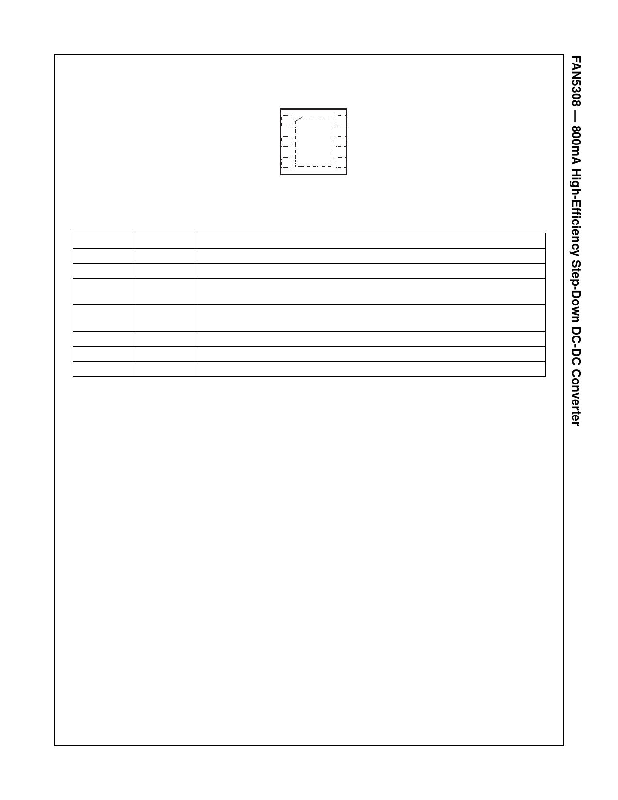
Pin Configuration
VIN 1
PGND 2
P1
(AGND)
6 SW
5 NC
EN 3
4 FB
Pin Description
Pin #
P1
1
2
Name
AGND
VIN
PGND
3
EN
4
FB
5
NC
6
SW
Figure 2. Pin Assignment for 3x3mm 6-Lead MLP
Description
Analog Ground. P1 must be soldered to the PCB ground.
Supply Voltage Input.
Power Ground. This pin is connected to the internal MOSFET switches. This pin must
be externally connected to AGND.
Enable Input. Logic high enables the chip and logic low disables the chip, reducing
the supply current to less than 1µA. Do not float this pin.
Feedback Input. Adjustable voltage option, connect this pin to the resistor divider.
No Connection Pin.
Switching Node. This pin is connected to the internal MOSFET switches.
© 2005 Fairchild Semiconductor Corporation
FAN5308 Rev. 1.0.2
2
www.fairchildsemi.com
Share Link: 