GS71116AJ Ver la hoja de datos (PDF) - Unspecified
Número de pieza
componentes Descripción
Lista de partido
GS71116AJ Datasheet PDF : 15 Pages
| |||
GS71116ATP/J/U
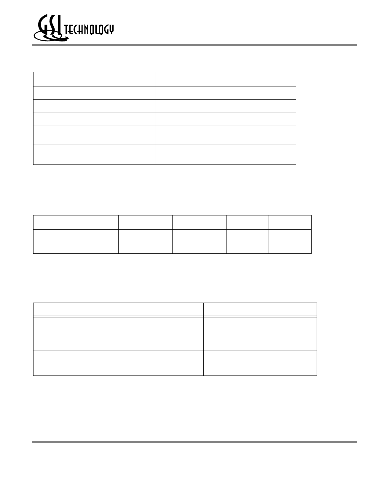
Recommended Operating Conditions
Parameter
Symbol Min
Typ
Supply Voltage for -7/-8/-10/-12
VDD
3.0
3.3
Input High Voltage
VIH
2.0
—
Input Low Voltage
VIL
–0.3
—
Ambient Temperature,
Commercial Range
TAc
0
—
Ambient Temperature,
Industrial Range
TAI
–40
—
Notes:
1. Input overshoot voltage should be less than VDD +2 V and not exceed 20 ns.
2. Input undershoot voltage should be greater than –2 V and not exceed 20 ns.
Max
3.6
VDD +0.3
0.8
70
85
Capacitance
Parameter
Input Capacitance
Output Capacitance
Symbol
Test Condition
Max
CIN
VIN = 0 V
5
COUT
VOUT = 0 V
7
Notes:
1. Tested at TA = 25°C, f = 1 MHz
2. These parameters are sampled and are not 100% tested.
DC I/O Pin Characteristics
Parameter
Symbol
Input Leakage Current
IIL
Output Leakage
Current
ILO
Output High Voltage
VOH
Output Low Voltage
VOL
Test Conditions
VIN = 0 to VDD
Output High Z
VOUT = 0 to VDD
IOH = –4 mA
ILO = +4 mA
Min
–1 uA
–1 uA
2.4
Unit
V
V
V
oC
oC
Unit
pF
pF
Max
1uA
1uA
0.4V
Rev: 1.04a 10/2002
4/15
© 2001, Giga Semiconductor, Inc.
Specifications cited are subject to change without notice. For latest documentation see http://www.gsitechnology.com.
Share Link: 