HIP6019B(1998) Ver la hoja de datos (PDF) - Intersil
Número de pieza
componentes Descripción
Lista de partido
HIP6019B Datasheet PDF : 15 Pages
| |||
HIP6019B
TABLE 1.
VID4
PIN NAME
VID3
VID2
VID1
VID0
NOMINAL
OUT1
VOLTAGE
DACOUT
1
1
1
1
1
INHIBIT
1
1
1
1
0
2.1
1
1
1
0
1
2.2
1
1
1
0
0
2.3
1
1
0
1
1
2.4
1
1
0
1
0
2.5
1
1
0
0
1
2.6
1
1
0
0
0
2.7
1
0
1
1
1
2.8
1
0
1
1
0
2.9
1
0
1
0
1
3.0
1
0
1
0
0
3.1
1
0
0
1
1
3.2
1
0
0
1
0
3.3
1
0
0
0
1
3.4
1
0
0
0
0
3.5
NOTE: 0 = connected to GND or VSS, 1 = open or connected to 5V
through pull-up resistors.
Layout Considerations
MOSFETs switch very fast and efficiently. The speed with
which the current transitions from one device to another
causes voltage spikes across the interconnecting
impedances and parasitic circuit elements. The voltage
spikes can degrade efficiency, radiate noise into the circuit,
and lead to device over-voltage stress. Careful component
layout and printed circuit design minimizes the voltage
spikes in the converter. Consider, as an example, the turnoff
transition of the upper MOSFET. Prior to turnoff, the upper
MOSFET was carrying the full load current. During the
turnoff, current stops flowing in the upper MOSFET and is
picked up by the lower MOSFET or Schottky diode. Any
inductance in the switched current path generates a large
voltage spike during the switching interval. Careful
component selection, tight layout of the critical components,
and short, wide circuit traces minimize the magnitude of
voltage spikes. Contact Intersil for evaluation board
drawings of the component placement and printed circuit
board.
There are two sets of critical components in a DC-DC converter
using a HIP6019B controller. The power components are the
most critical because they switch large amounts of energy. The
critical small signal components connect to sensitive nodes or
supply critical bypassing current.
The power components should be placed first. Locate the
input capacitors close to the power switches. Minimize the
length of the connections between the input capacitors and
the power switches. Locate the output inductor and output
capacitors between the MOSFETs and the load. Locate the
PWM controller close to the MOSFETs.
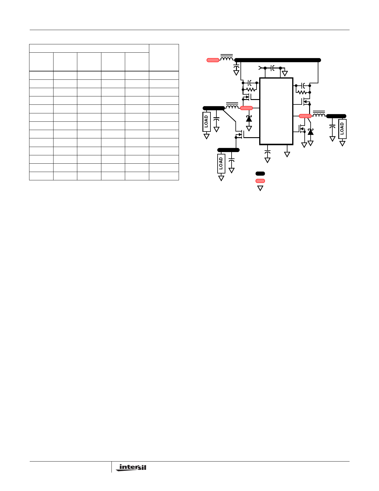
+5VIN
VOUT2
CIN
+12V
COCSET2 CVCC
VCC GND
COCSET1
ROCSET2
OCSET2 OCSET1
ROCSET1
Q3
LOUT2
UGATE2
Q1
UGATE1
PHASE2
LOUT1
PHASE1
VOUT1
COUT2
Q4
VOUT3
HIP6019B Q2
LGATE1
GATE3
SS
PGND
COUT1
CR1
CSS
KEY
ISLAND ON POWER PLANE LAYER
ISLAND ON CIRCUIT PLANE LAYER
VIA CONNECTION TO GROUND PLANE
FIGURE 10. PRINTED CIRCUIT BOARD POWER PLANES AND
ISLANDS
The critical small signal components include the bypass
capacitor for VCC and the soft-start capacitor, CSS. Locate
these components close to their connecting pins on the
control IC. Minimize any leakage current paths from SS
node because the internal current source is only 11µA.
A multi-layer printed circuit board is recommended. Figure 10
shows the connections of the critical components in the
converter. Note that capacitors CIN and COUT could each
represent numerous physical capacitors. Dedicate one solid
layer for a ground plane and make all critical component
ground connections with vias to this layer. Dedicate another
solid layer as a power plane and break this plane into smaller
islands of common voltage levels. The power plane should
support the input power and output power nodes. Use copper
filled polygons on the top and bottom circuit layers for the
phase nodes. Use the remaining printed circuit layers for
small signal wiring. The wiring traces from the control IC to the
MOSFET gate and source should be sized to carry 1A
currents. The traces for OUT4 need only be sized for 0.2A.
Locate COUT4 close to the HIP6019B IC.
PWM Controller Feedback Compensation
Both PWM controllers use voltage-mode control for output
regulation. This section highlights the design consideration
for a voltage-mode controller. Apply the methods and
considerations to both PWM controllers.
Figure 11 highlights the voltage-mode control loop for a
synchronous-rectified buck converter. The output voltage is
regulated to the reference voltage level. The reference
voltage level is the DAC output voltage for PWM1 and is
1.265V for PWM2. The error amplifier output (VE /A) is
276
Share Link: 