HIP6020A(1999) Ver la hoja de datos (PDF) - Intersil
Número de pieza
componentes Descripción
Lista de partido
HIP6020A Datasheet PDF : 16 Pages
| |||
HIP6020A
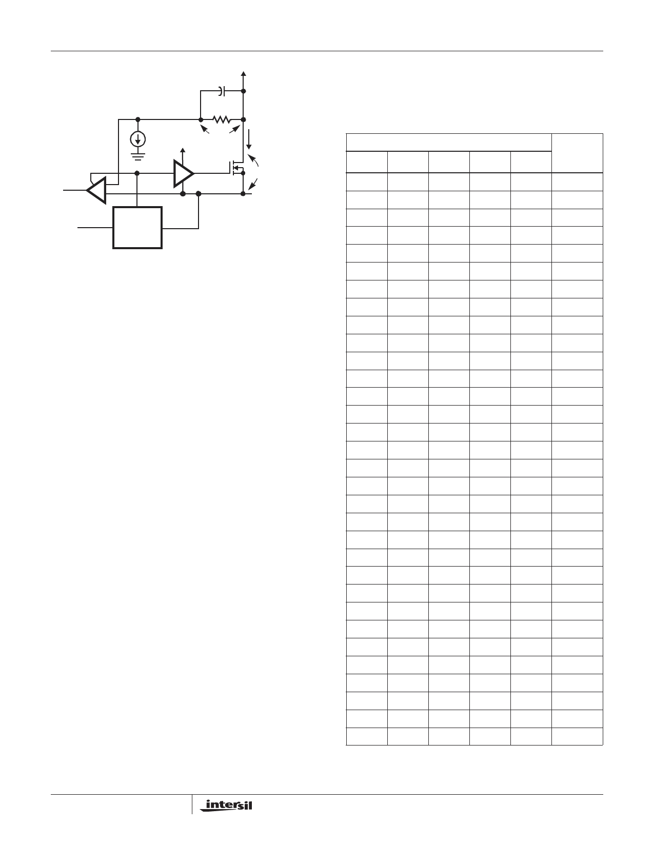
OVER-CURRENT TRIP:
VDS > VSET
iD × rDS(ON) > IOCSET × ROCSET
OCSET
VIN = +5V
ROCSET
OVER-
CURRENT
OC
+
-
IOCSET
200µA
DRIVE
VSET +
VCC
UGATE
PHASE
iD
+
VDS
PWM
GATE
CONTROL
VPHASE = VIN – VDS
VOCSET = VIN – VSET
FIGURE 6. OVER-CURRENT DETECTION
Resistors (ROCSET1 and ROCSET2) program the over-current
trip levels for each PWM converter. As shown in Figure 9, the
internal 200µA current sink (IOCSET) develops a voltage across
ROCSET (VSET) that is referenced to VIN. The DRIVE signal
enables the over-current comparator (OVER-CURRENT1 or
OVER-CURRENT2). When the voltage across the upper
MOSFET (VDS(ON)) exceeds VSET, the over-current
comparator trips to set the over-current latch. Both VSET and
VDS are referenced to VIN and a small capacitor across
ROCSET helps VOCSET track the variations of VIN due to
MOSFET switching. The over-current function will trip at a peak
inductor current (IPEAK) determined by:
IPEAK = I--O-----C----S----Er--D--T---S--×--(--OR----N-O---)-C-----S----E---T--
The OC trip point varies with MOSFET’s rDS(ON)
temperature variations. To avoid over-current tripping in the
normal operating load range, determine the ROCSET
resistor value from the equation above with:
1. The maximum rDS(ON) at the highest junction temperature
2. The minimum IOCSET from the specification table
3. Determine IPEAK for IPEAK > IOUT(MAX) + (∆I) / 2,
where ∆I is the output inductor ripple current.
For an equation for the ripple current see the section under
component guidelines titled ‘Output Inductor Selection’.
OUT1 Voltage Program
The output voltage of the PWM1 converter is programmed to
discrete levels between 1.3VDC and 3.5VDC. This output
(OUT1) is designed to supply the core voltage of Intel’s
advanced microprocessors. The voltage identification (VID)
pins program an internal voltage reference (DACOUT) with a
TTL-compatible 5-bit digital-to-analog converter (DAC). The
level of DACOUT also sets the PGOOD and OVP thresholds.
Table 1 specifies the DACOUT voltage for the different
combinations of connections on the VID pins. The VID pins
can be left open for a logic 1 input, because they are internally
pulled up to an internal voltage of about 5V by a 10µA current
source. Changing the VID inputs during operation is not
recommended and could toggle the PGOOD signal and
exercise the over-voltage protection.
OUT2 Voltage Selection
The AGP regulator output voltage is internally set to 1.5V or
continuously on, based on the status of the SELECT pin.
SELECT pin is internally pulled ‘high’, such that left open,
the standard buck MOSFET will be continuously on, VOUT2
being equal to the input voltage (3.3V) less any voltage drop
across the MOSFET’s rDS(ON) and output inductor’s DCR.
The other setting available is 1.5V, which can be obtained by
grounding the SELECT pin using a jumper or another
suitable method capable of sinking a few tens of
microamperes. The status of the SELECT pin cannot be
changed during operation of the IC without possibly causing
a fault condition.
VID4
0
0
0
0
0
0
0
0
0
0
0
0
0
0
0
0
1
1
1
1
1
1
1
1
1
1
TABLE 1. OUT1 VOLTAGE PROGRAM
PIN NAME
VID3 VID2 VID1
VID0
NOMINAL
DACOUT
VOLTAGE
1
1
1
1
1.30
1
1
1
0
1.35
1
1
0
1
1.40
1
1
0
0
1.45
1
0
1
1
1.50
1
0
1
0
1.55
1
0
0
1
1.60
1
0
0
0
1.65
0
1
1
1
1.70
0
1
1
0
1.75
0
1
0
1
1.80
0
1
0
0
1.85
0
0
1
1
1.90
0
0
1
0
1.95
0
0
0
1
2.00
0
0
0
0
2.05
1
1
1
1
2.00
1
1
1
0
2.1
1
1
0
1
2.2
1
1
0
0
2.3
1
0
1
1
2.4
1
0
1
0
2.5
1
0
0
1
2.6
1
0
0
0
2.7
0
1
1
1
2.8
0
1
1
0
2.9
4-9
Share Link: 