HS-303CEH Ver la hoja de datos (PDF) - Intersil
Número de pieza
componentes Descripción
Lista de partido
HS-303CEH Datasheet PDF : 10 Pages
| |||
HS-303CEH
Absolute Maximum Ratings
Voltage Between V+ and V- Terminals . . . . . . . . . . . . . . . . . . . . . . . . . . . 35V
±VSUPPLY to Ground (V+, V-) . . . . . . . . . . . . . . . . . . . . . . . . . . . . . . . . .±17.5V
Analog Input Voltage
(+VS). . . . . . . . . . . . . . . . . . . . . . . . . . . . . . . . . . . . . . . . . . .+VSUPPLY +1.5V
(-VS) . . . . . . . . . . . . . . . . . . . . . . . . . . . . . . . . . . . . . . . . . . . . -VSUPPLY -1.5V
Digital Input Voltage
(+VA) . . . . . . . . . . . . . . . . . . . . . . . . . . . . . . . . . . . . . . . . . . . . +VSUPPLY +4V
(-VA) . . . . . . . . . . . . . . . . . . . . . . . . . . . . . . . . . . . . . . . . . . . . . . -VSUPPLY -4V
Peak Current (S or D)
(Pulse at 1ms, 10% Duty Cycle Max) . . . . . . . . . . . . . . . . . . . . . . . . 40mA
Continuous Current . . . . . . . . . . . . . . . . . . . . . . . . . . . . . . . . . . . . . . . . 10mA
Thermal Information
Thermal Resistance (Typical)
θJA (°C/W) θJC (°C/W)
Flatpack Package (Notes 1, 2) . . . . . . . . . . 105
17
Package Power Dissipation at 125°C
Flatpack Package. . . . . . . . . . . . . . . . . . . . . . . . . . . . . . . . . . . . 0.48W/°C
Lead Temperature (Soldering, 10s) . . . . . . . . . . . . . . . . . . . . . . . . . . . 300°C
Junction Temperature (TJ) . . . . . . . . . . . . . . . . . . . . . . . . . . . . . . . . . .+175°C
Storage Temperature Range. . . . . . . . . . . . . . . . . . . . . . . .-65°C to +150°C
Pb-Free Reflow Profile . . . . . . . . . . . . . . . . . . . . . . . . . . . . . . . see link below
http://www.intersil.com/pbfree/Pb-FreeReflow.asp
Recommended Operating Conditions
Operating Temperature Range . . . . . . . . . . . . . . . . . . . . . .-55°C to +125°C
Operating Supply Voltage Range (±VSUPPLY) . . . . . . . . . . . . . . . . . . . . ±15V
Analog Input Voltage (VS) . . . . . . . . . . . . . . . . . . . . . . . . . . . . . . . . ±VSUPPLY
Logic Low Level (VAL) . . . . . . . . . . . . . . . . . . . . . . . . . . . . . . . . . . . .0V to 0.8V
Logic High Level (VAH) . . . . . . . . . . . . . . . . . . . . . . . . . . . . .4.0V to +VSUPPLY
CAUTION: Do not operate at or near the maximum ratings listed for extended periods of time. Exposure to such conditions may adversely impact product
reliability and result in failures not covered by warranty.
NOTES:
1. θJA is measured with the component mounted on a low effective thermal conductivity test board in free air. See Tech Brief TB379 for details.
2. For θJC, the “case temp” location is the center of the package underside.
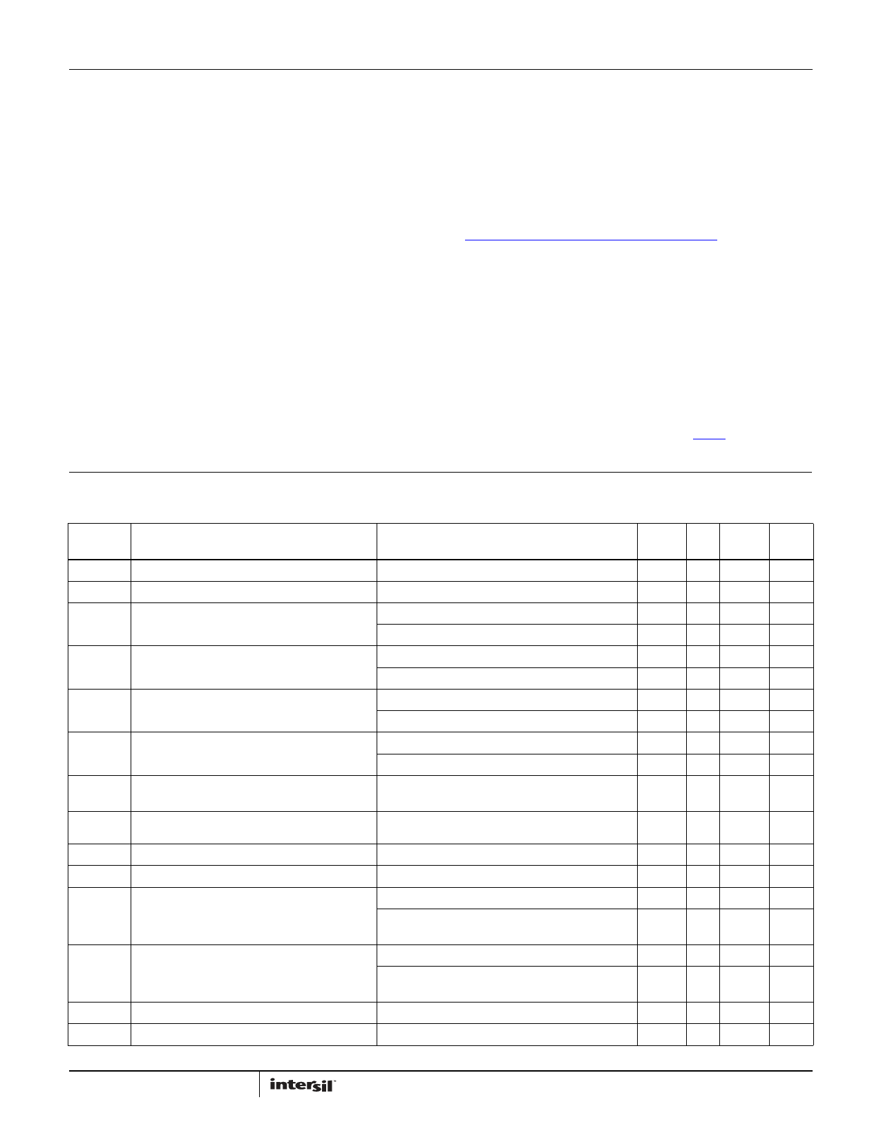
Electrical Specifications VSUPPLY = ±15V unless otherwise specified. Boldface limits apply across the operating temperature range,
-55°C to +125°C.
SYMBOL
PARAMETER
TEST CONDITIONS
MIN
MAX
(Note 5) TYP (Note 5) UNITS
+rDS(ON)
-rDS(ON)
+IS(OFF)
-IS(OFF)
+ID(OFF)
-ID(OFF)
+ID(ON)
“Switch On” Resistance
VD = 10V, IS = -10mA
“Switch On” Resistance
VD = -10V, IS = 10mA
Leakage Current into Source of an “OFF” Switch VS = +14V, VD = -14V
VS = +15V, VD = -15V
Leakage Current into Source of an “OFF” Switch VS = -14V, VD = +14V
VS = -15V, VD = +15V
Leakage Current into Drain of an “OFF” Switch VS = +14V, VD = -14V
VS = +15V, VD = -15V
Leakage Current into Drain of an “OFF” Switch VS = -14V, VD = +14V
VS = -15V, VD = +15V
Leakage Current from an “ON” Driver into the
Switch (Drain and Source)
VS = +14V, VD = +14V
35 75
Ω
35 75
Ω
-150 0.05 150
nA
-20
20
µA
-150 0.5 150
nA
-20
20
µA
-150 0.05 150
nA
-20
20
µA
-150 0.5 150
nA
-20
20
µA
-100 -0.1 100
nA
-ID(ON)
IAL
IAH
I+
Leakage Current from an “ON” Driver into the
Switch (Drain and Source)
Low Level Input Address Current
High Level Input Address Current
Positive Supply Current
I-
Negative Supply Current
CIS(OFF) Switch Input Capacitance
VS = -14V, VD = -14V
All Channels VA = 0.8V
All Channels VA = 4.0V
All Channels VA = 0.8V
VA1 = 0V, VA2 = 4V
VA1 = 4V, VA2 = 0V
All Channels VA = 0.8V
VA1 = 0V, VA2 = 4V
VA1 = 4V, VA2 = 0V
From Source to GND (Notes 3, 4)
-100 0.01 100
nA
-1000 0.03 1000 nA
-1000 0.03 1000 nA
45 150
µA
0.15 0.6
mA
-0.1 -100 µA
-0.1 -100 µA
28
pF
CC1 Driver Input Capacitance
VA = 0V (Notes 3, 4)
10
pF
3
FN8399.1
April 19, 2013
Share Link: 