HSP50214 Ver la hoja de datos (PDF) - Intersil
Número de pieza
componentes Descripción
Lista de partido
HSP50214 Datasheet PDF : 54 Pages
| |||
HSP50214
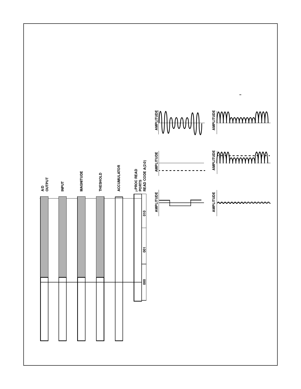
The integration period counter can be set up to run
continuously or to count down and stop. Continuous
integration counter operation lets the counter run, with
sampling occurring every time the counter reaches zero.
Because the processor samples the detector read port
asynchronous to the CLKIN, data can be missed unless the
status bit is monitored by the processor to ensure that a
sample is taken for every integration count down sequence.
In the count down and stop mode, the microprocessor read
commands can be synchronized to system events, such as
the start of a burst for a TDMA application. The integration
counter can be started at any time by writing to Control Word
2. At the end of the integration period (counter = 0000), the
upper 23 bits of the accumulator are transferred to a holding
register for reading by the microprocessor. Note that it is not
the restarting of the counter (by writing to Control Word 2)
that latches the current value, but the end of the integration
count. When the accumulator results are latched, a bit is set
in the status register to notify the processor. Reading the
most significant byte of the 23 bits clears the status bit. See
the Microprocessor Read Section. Figure 11 illustrates a
typical AGC detection process.
Typically, the average input error is read from the Input Level
Detector port for use in AGC applications. By setting the
threshold to 0, however, the average value of the input signal
can be read directly. The calculation is:
dBFSRMS = (20)log [(1.111)(leve l) ⁄ ((N)(16))]
(EQ. 2)
where “level” is the 24-bit value read from the 3 level detec-
tor registers and “N” is the number of samples to be inte-
grated. Note that to get the average value of a sinusoid,
multiply the RMS value by 1.111. For a full scale input sinu-
soid, this yields an RMS value of approximately 3dBFS.
NOTE: 1.111 scales the sinusoid average (2/π) to 1/√2
.
A) INPUT SIGNAL
B) RECTIFIED SIGNAL
C) THRESHOLD
D) ACCUMULATOR INPUTS
0
218
218
217
217
216
216
215
215
214
214
213
213
212
212
211
211
210
210
29
29
28
28
27
27
26
26
25
25
24
24
23
23
22
22
f
S
20
20
0
21
21
-20
20
20
-6dB 2-1
2-1
2-1
2-1
2-1
2-1
-12dB 2-2
2-2
2-2
2-2
2-2
2-2
-18dB
-24dB
-30dB
-36dB
2-3
2-4
2-5
2-3
2-4
2-5
2-3
2-4
2-5
2-3
2-4
2-5
2-3
2-4
2-5
2-3
2-4
-42dB 2-6
2-6
2-6
2-6
2-6
-48dB 2-7
2-7
2-7
2-7
2-7
-54dB 2-8
2-8
2-8
2-8
2-8
-60dB 2-9
2-9
2-9
2-9
2-9
-66dB
-72dB
-78dB
-84dB
2-10
2-11
2-12
2-10
2-11
2-12
2-10
2-11
2-12
2-10
2-11
2-12
2-10
2-11
2-12
-90dB 2-13
2-13
2-13
2-13
2-13
FIGURE 10. INPUT THRESHOLD DETECTOR BIT WEIGHTING
E) DETECTOR OUTPUT
F) CLOSED LOOP STEADY STATE
(CONSTANT INPUT)
FIGURE 11. SIGNAL PROCESSING WITHIN LEVEL DETECTOR
Carrier Synthesizer/Mixer
The carrier synthesizer/mixer section of the HSP50214 is
shown in Figure 12. The NCO has a 32-bit phase accumula-
tor, a 10-bit phase offset adder, and a sine/cosine ROM.
The frequency of the NCO is the sum of a center frequency
control word, loaded via the microprocessor interface (Con-
trol Word 3, bits 0 to 31), and an offset frequency, loaded
serially via the COF and COFSYNC pins. The offset fre-
quency can be zeroed in Control Word 0, bit 1. Both fre-
quency control terms are 32 bits and the addition is modulo
232. The output frequency of the NCO is computed as:
FC = fIN* N ⁄ (232) ,
or in terms of the programmed value:
(EQ. 3)
N = INT[FC × 232 ⁄ FIN]HEX ,
(EQ. 3A)
where N is the 32-bit sum of the center and offset frequency
terms, fIN is the input sampling frequency, and INT is the
integer of the computation. See the Microprocessor Write
Section on instructions for writing Control Word 3.
11
Share Link: 