HT1647A Ver la hoja de datos (PDF) - Holtek Semiconductor
Número de pieza
componentes Descripción
Lista de partido
HT1647A Datasheet PDF : 19 Pages
| |||
PATENTED
HT1647A
Pad No.
11
12
13
14
15
16
17
18
19
20
21
22
23
24
25
26
27
28
29
30
31
32
33
34
X
-1512.50
-1512.50
-1512.50
-1512.50
-1512.50
-1512.50
-1512.50
-1512.50
-1512.50
-1512.50
-1512.50
-1512.50
-1441.90
-1441.90
-1441.90
-1240.80
-1145.80
-1040.20
-945.20
-842.00
-743.30
-637.70
-542.70
-437.10
Y
101.25
6.25
-88.75
-183.75
-278.75
-373.75
-468.75
-563.75
-658.75
-753.75
-848.75
-943.75
-1095.00
-1190.00
-1295.60
-1310.40
-1310.40
-1310.40
-1310.40
-1310.40
-1310.40
-1310.40
-1310.40
-1310.40
Pad No.
45
46
47
48
49
50
51
52
53
54
55
56
57
58
59
60
61
62
63
64
65
66
67
68
X
781.30
876.30
971.30
1066.30
1161.30
1256.30
1351.30
1446.30
1512.50
1512.50
1512.50
1512.50
1512.50
1512.50
1512.50
1512.50
1512.50
1512.50
1512.50
1512.50
1512.50
1512.50
1512.50
1512.50
Y
-1410.00
-1410.00
-1410.00
-1410.00
-1410.00
-1410.00
-1410.00
-1410.00
-949.55
-845.55
-759.55
-664.55
-569.55
-474.55
-379.55
-284.55
-166.15
-71.15
23.85
118.85
213.85
308.85
403.85
498.85
Pad No.
79
80
81
82
83
84
85
86
87
88
89
90
91
92
93
94
95
96
97
98
99
100
101
102
X
900.60
805.60
710.60
615.60
520.60
425.60
330.60
235.60
140.60
45.60
-49.40
-144.40
-239.40
-334.40
-429.40
-524.40
-619.40
-714.40
-809.40
-904.40
-999.40
-1094.40
-1189.40
-1284.40
Y
1407.45
1407.45
1407.45
1407.45
1407.45
1407.45
1407.45
1407.45
1407.45
1407.45
1407.45
1407.45
1407.45
1407.45
1407.45
1407.45
1407.45
1407.45
1407.45
1407.45
1407.45
1407.45
1407.45
1407.45
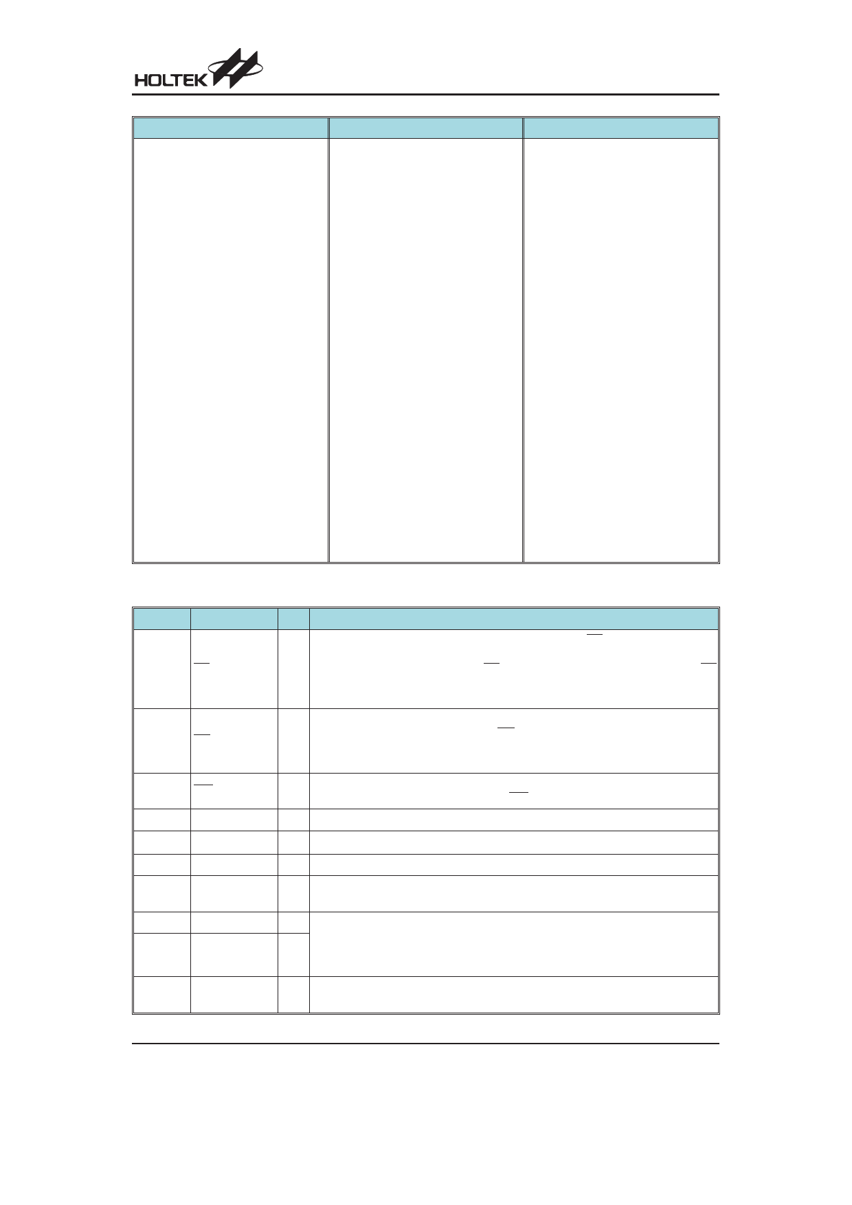
Pad Description
Pad No. Pad Name
23
CS
24
RD
25
WR
26~29
30
31
DB0~DB3
VSS
OP1
32
OP2
33
OSCI
34
OSCO
35
OP3
I/O
Description
Chip selection input with pull-high resistor. When the CS is logic high, the data
and command read from or write to the HT1647A are disabled. The serial inter-
I face circuit is also reset. But if the CS is at a logic low level and is input to the CS
pad, the data and command transmission between the host controller and the
HT1647A are all enabled.
READ clock input with pull-high resistor. Data in the RAM of the HT1647A are
I
clocked out on the rising edge of the RD signal. The clocked out data will appear
on the data line. The host controller can use the next falling edge to latch the
clocked out data.
I
WRITE clock input with pull-high resistor. Data on the DATA line are latched into
the HT1647A on the rising edge of the WR signal.
I/O Parallel data input/output with a pull-high resistor
¾ Negative power supply for logic circuit, ground
I Used to select D3, D1 or D2, D0; OP1 input with pull-low resistor.
I
OP2 and OP3 are used to select two of four level gray scale; OP2 input with
pull-high resistor.
I The OSCI and OSCO pads are connected to a 32.768kHz crystal in order to gen-
erate a system clock. If the system clock comes from an external clock source, the
O external clock source should be connected to the OSCI pad. But if an on-chip RC
oscillator is selected, the OSCI and OSCO pads can be left open.
I
OP2 and OP3 are used to select two of four level gray scale ; OP3 input with
pull-high resistor.
Rev. 1.40
4
April 29, 2011
Share Link: 